
 NextPCB Capabilities
Printed Circuit Boards
NextPCB Capabilities
Printed Circuit Boards
 PCB Assembly
 Layer Buildup
 SMD-Stencils
 PCB Design-Aid & Layout
 Mechanics
 Quality
 Drills & Throughplating
 Factory & Certificate
 PCB Assembly Factory Show
Certificate
PCB Assembly Factory Show
Certificate
Support Team
Feedback:
support@nextpcb.com


In most electronics, the surface-mounted and socketed components get physically supported and wiring with the help of a printed circuit board (PCB).
PCBs are created using a photolithographic method, which is a scaled-up replica of how conductive routes in processors are created, for use in applications that require delicate conductive traces, such as computers.
On a finished PCB with solder dabs in place, electronic components normally mount with the use of a special machine. In an industrial oven, the PCB bakes to melt the solder connecting the connections. The majority of PCBs constructs with the use of copper traces from fibreglass or glass-reinforced polymers.
For simple electronic devices, single-layer PCBs are an option. Printed circuit boards with sophisticated hardware, such as motherboards and graphics cards, can contain up to twelve layers. PCBs can be any color, although they are most frequently green.
When comes to the mini PCB, spending money and time on ordering it from the industry is a huge waste. Instead of that, you can make your own PCB at home. This will save you money and time. Since you are getting the experience you will be well-trained in designing PCB at home. Since you are the designer and the manufacturer, you can customize the PCB as you want without limitation.
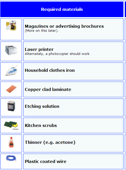
Just a few supplies and tools are required, including a PCB board, a bottle of ferric chloride, a little drill, a small container, a bottle of thinner, and some plastic tweezers. Making your own circuit board is simple and only takes 30 to 45 minutes.
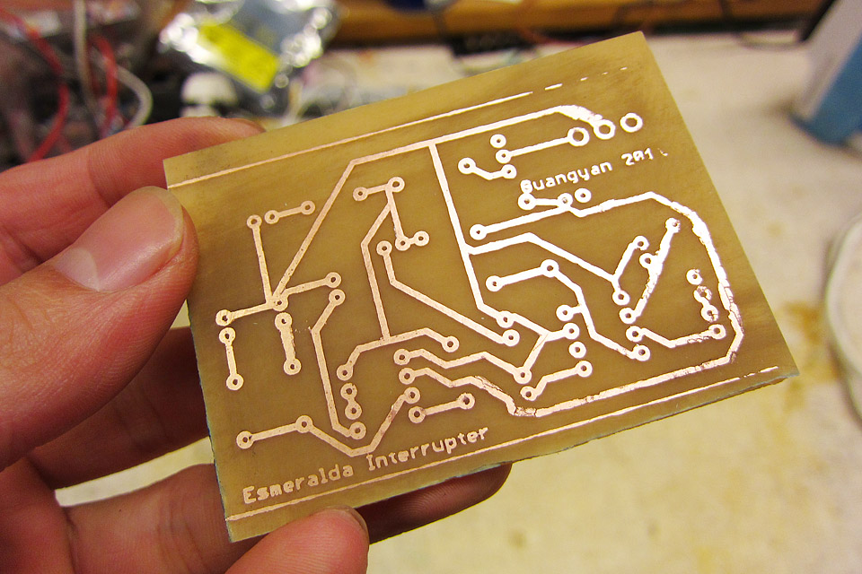
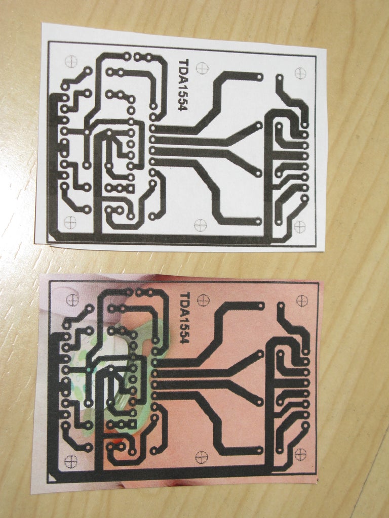
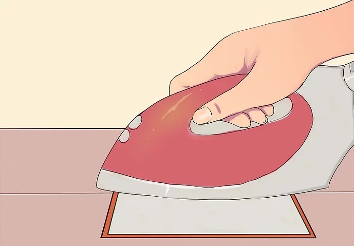
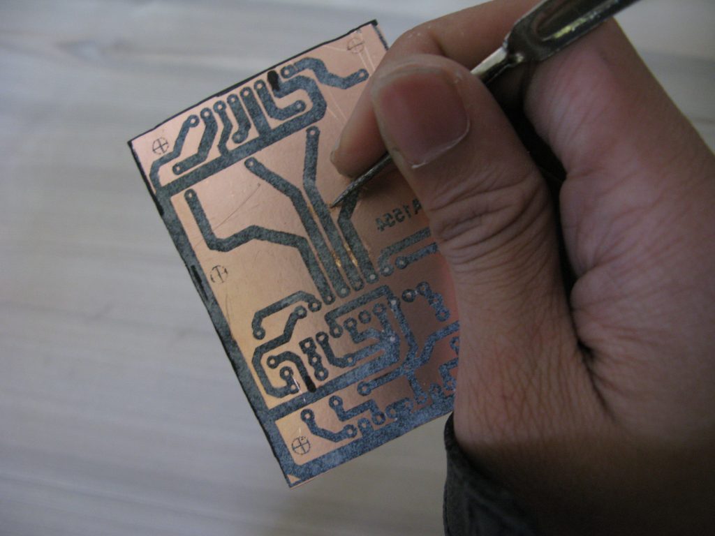
Typically, you print your circuit design on glossy paper, photo paper, or magazine paper and attach it in directly to your board. Let me remind you that using an inkjet printer won't work; you must use a laser printer or a photocopier before printing. Your printed circuit board design should be ironed over the copper side of the printed circuit board (PCB) once it has been printed. This will transfer the ink from the glossy paper to the PCB board. The copper component that shouldn't be etched is protected by the ink as a layer.
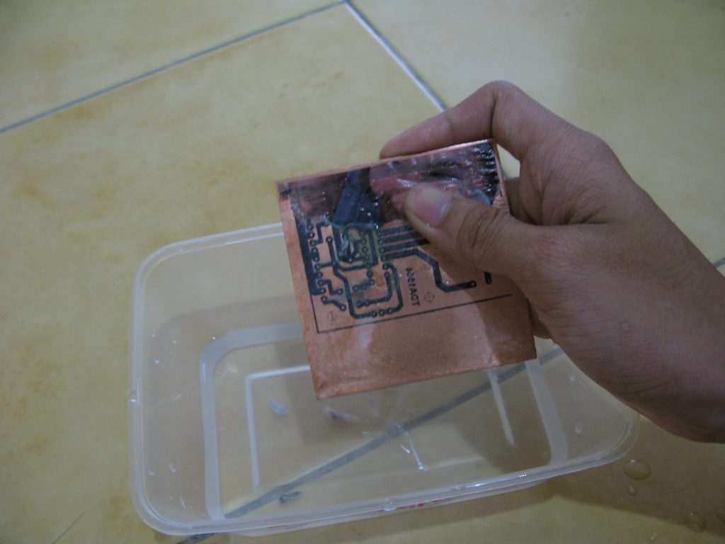
After applying the ink to the PCB board, you will need to dip the PCB board for 15 minutes in an etching solution like ferric chloride. You might need to wash the PCB board with water after etching it to get rid of the etching solution. To reveal the uneched copper section, use thinner to remove any leftover ink after rinsing. Drill holes on the board so that your components can be soldered there when the ink has been removed. Last but not least, finish your personalized board by simply soldering the components on it.
You have to be very conscious about every step of this process. So, in the end, you will get a good product safely.
If you already have a PCB layout, there won't be any issues; just move on to the next stage. If you don't have any plans for using the printing method, you might as well write your design directly on the board. You should first create your own PCB layout before making your own customized PCB board. Making your own PCB layout is possible with the aid of good PCB designing software.
The most complete, cutting-edge, end-to-end PCB design software is Altium Designer, which is also the most popular option among engineers and designers worldwide. Altium Designer gives out a totally unified design environment. This represents decades of innovation and development and unites teams from around the world with all facets of the PCB design process.
For product designers, mechanical engineers, electronics engineers, and machinists, Fusion 360 is the first and only complete cloud CAD, CAM, CAE, and PCB product development solution. It enables you to link your whole design to the manufacturing product development process, accelerating the time it takes to bring high-quality items to market and improving your bottom line. It is available for PC and Mac and features advanced simulation, 2.5, 3, 4, and 5-axis machining, and generative design.
Electronic design automation (EDA) software is available from Autodesk. enabling the seamless integration of schematic designs, component placement, PCB routing, and extensive library content for printed circuit board (PCB) designers.
SOLIDWORKS PCB allows both the innovative collaboration between electrical and 3D mechanical design teams and the productivity you need to develop Printed Circuit Boards (PCBs) quickly. It provides a glaring advantage in the area where successful ECAD-MCAD collaboration is essential for the overall design of electronic products.
The use of any of the above software will gain the potential to design your PCB design very neat and clean.
We must first define the word "PCB layout," which you will hear frequently. It is a CAD drawing that displays every component's placement on constructed printed circuit boards. All parts and copper that will be visible on both sides of a PCB are included in this.
Contrast this with a printed wiring board design, which resembles a PCB layout but this undergoes without the addition of any electrical components.
Use a laser printer or a photocopier to print your layout; inkjet printers won't work because their ink is soluble in water and won't transfer its ink to the PCB board. try to use any glossy paper you like; magazine sheets will do.
The following things to keep in mind:
After printing, be careful not to touch the ink because it can get on your hands.
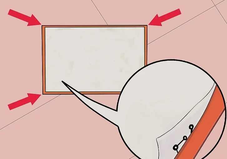
The alignment of the paper with the board is very important. This will give you a clear and good PCB. Mainly when come to the spacing, the correct alignment of the design really matters. This step is basically to make your PCB looks nicer.
You have to submerge the board in a container of tap water for two to five minutes. Otherwise, it is possible to rub while being exposed to running water from the sink. To prevent the ink from being erased when you rub the paper off the board, wait until it becomes soggy before gently rubbing.
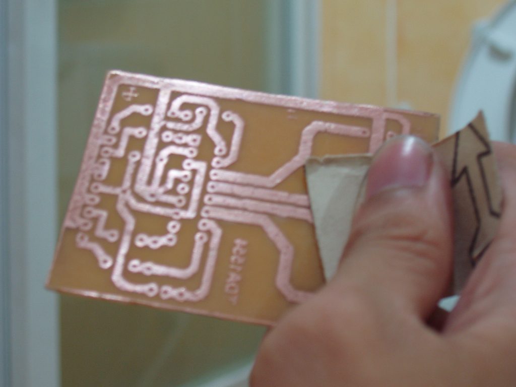
Once the board get the print on it, next you have to make the board much more professional. For that, you have to remove the excess parts of the board by using a hack saw. this will make the board appropriate to the design on the board. Moreover, it will make the board eye-catching.
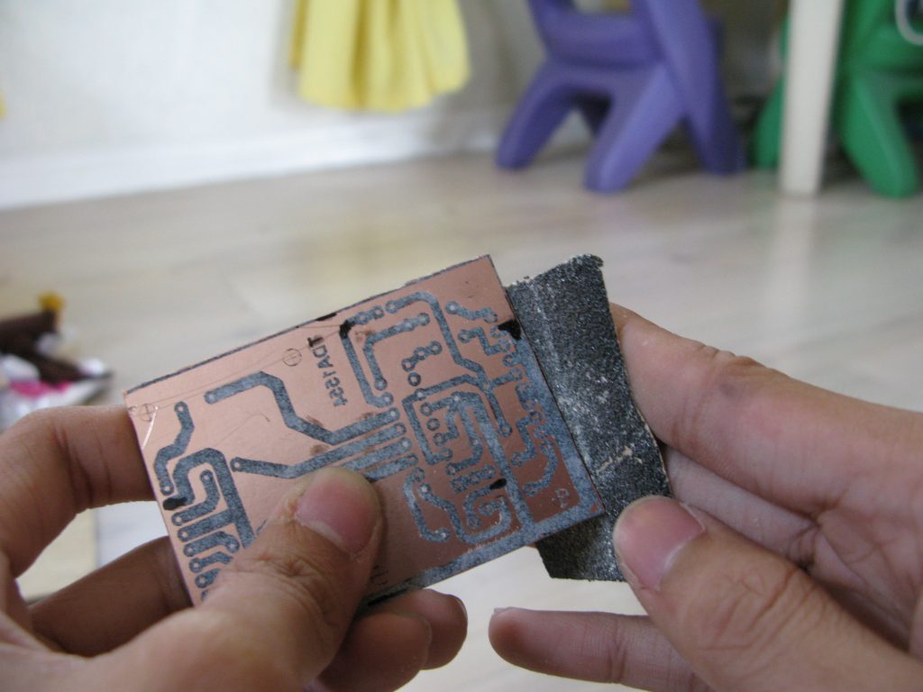
Next for safety, you have to smooth the edges of the board using sandpaper. In this step, be aware of the damaging the drawing on the board. applying a huge force on the sandpaper may damage the board and destroy your drawing.
There will still be the excess paper on the board even after you have rubbed the paper off; to remove it, use a very sharp instrument, such as the cutter's tip, the point of a sharp compass, or a toothpick. You should use a marker and a ruler to repair any inked portions that were accidentally removed when you rubbed it off or sawed the excess board.
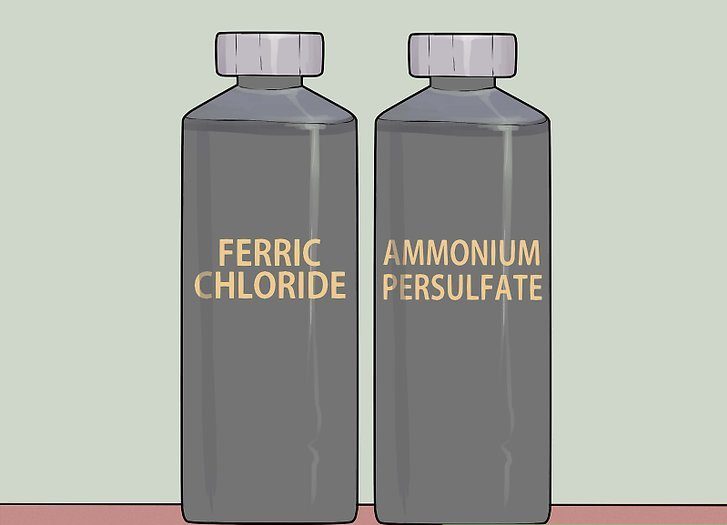
Example acids for the etching Ferric chloride is a typical etchant option. Crystals of ammonium persulfate or other chemical solutions can be used, though. No matter the chemical etchant you choose, it will always be dangerous, so in addition to taking the standard safety measures indicated in this article, you should read and abide by any specific safety instructions that come with the etchant.
There may be extra instructions, depending on the acid etch you select. For instance, certain crystalline acids must be dissolved in hot water, whilst other etchants can be used immediately.
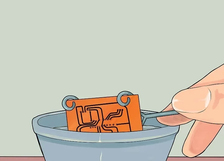
In this step, you have to submerge the board in the acid mixture. Keep the PCB submerged in the acid for 3 - 5 minutes. This will etch away the excess copper parts from the board. After keeping it submerged, take the board out and wait till the excess acid to remove from the surface of the board. Next, clean the paths of the board using a cotton bud.
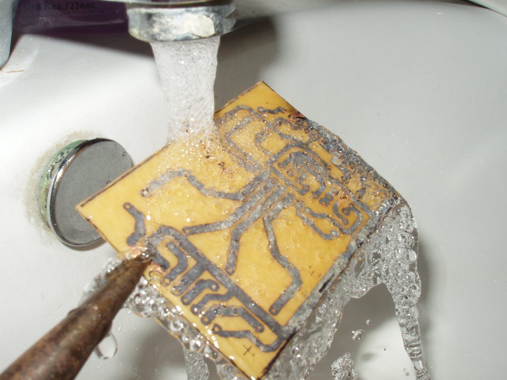
After the PCB board has been etched in the solution, rinse it with tap water. Wear gloves when cleaning it, please. To avoid having your tool become rusty like mine, it is advisable to use plastic tweezers rather than metallic ones like pliers.
After etching the board to reveal the copper portion of the board, you should first brush any remaining ink with laundry soap, or you might clean it with a small piece of fine sandpaper while giving it its shiny finish.
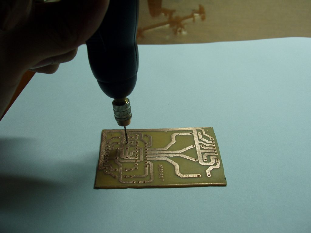
Use a small drill or Dremel tool to drill the board. After drilling it, give it another water rinse. Because the copper arrangement will serve as your drilling guide, make sure you drill it on the copper side. The drilling of the PCB should be according to the design you created.
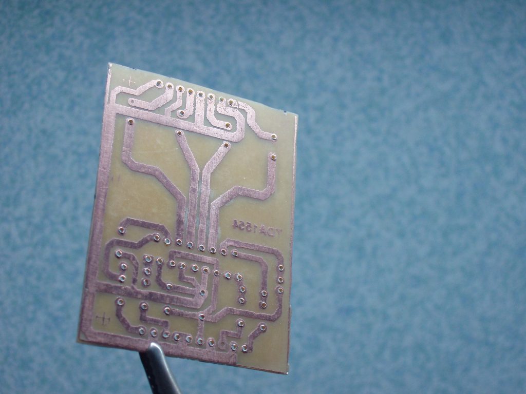
After following the all steps according to the mentioned way, in the end you will gain a PCB.
You can get a homemade own PCB, once the cleaning is over you can start the soldering of the components to the board. The components that select for these should be THT. Moreover, when you are following the above-mentioned approach please wear the necessary safety guards because you may handle the acids.
Still, need help? Contact Us: support@nextpcb.com
Need a PCB or PCBA quote? Quote now


 Surface

