
 NextPCB Capabilities
Printed Circuit Boards
NextPCB Capabilities
Printed Circuit Boards
 PCB Assembly
 Layer Buildup
 SMD-Stencils
 PCB Design-Aid & Layout
 Mechanics
 Quality
 Drills & Throughplating
 Factory & Certificate
 PCB Assembly Factory Show
Certificate
PCB Assembly Factory Show
Certificate
Support Team
Feedback:
support@nextpcb.com


Not long ago, people realized that printed circuit board wiring as a "stable technology" has gradually stagnated and become an obstacle to development. According to most people's opinion, the key part of the wiring has been solved, and the remaining problem is an inconvenience. Apart from that, there is nothing more to be exact. In the field of circuit board design and the development of the corresponding software tools involved, when technology enters a stable period, authorities will routinely use words such as "ordinary, dull" to describe it. Even industry experts with many years of experience advise and encourage PCB designers to constantly look for other real technical challenges.
Then, everything changed, which really surprised most people who stick to the rules. Gradually from the beginning to the present, with the development momentum of agglomeration, the field of PCB design is undergoing a huge change. Due to the collection of many key factors, including the rapid development of integrated circuit-related technologies, PCB designers need to reinvent their professional design work once again. Almost at the same time, the international authoritative analysis organization Dataquest put forward the "CAD revival" argument. And CAD obviously affects EDA design. A recent survey by Dataquest showed that despite the increasing importance of PCB layout tools in the past year, users are still dissatisfied with their performance. It can be seen that EDA suppliers must respond to this and provide a new generation of more advanced design tools, the core of which is naturally the PCB router.
In the past few years, technological innovation has shown unprecedented momentum, followed by rapid market adjustments. Whether it is computers, telecommunications, or consumer electronics, the pace of change is confusing and dizzying. Coupled with the stimulation of global competitive pressure, the advent of new products has become rapid and violent. A good example is that only one mobile phone manufacturer will launch a new model every three months, and sometimes many new products will be released within a year. To maintain this extremely fast speed means shortening the product design cycle and reducing costs. In order to successfully achieve the goal of reducing the design cycle, manufacturers must greatly increase their production capacity, because productivity is a nearly sacred goal in the technology market. At the same time, to achieve this goal, design tools must also be more effective and productive. However, the current situation is that PCB design tasks are usually completed at one time as planned, or at a high price. As people say, it’s not a bad thing to be fast.
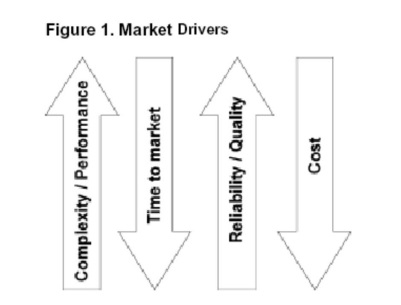
These major market forces drive the PCB design process and layout tools to become more productive in the shortest possible time.
Another outstanding development is that products are becoming more and more miniaturized. Suddenly, everything shrinks, from cellular phones, laptops, digital cameras to integrated circuits and the printed circuit boards that drive them. At the same time that the external dimensions tend to become smaller, more powerful functions and better performance are also urgently needed. In short, it is to be smaller, faster, more powerful, richer, and more reliable at the same time. No wonder now that PCB designers are facing more and more challenges. Now, more than ever, designers rely on better software tools to contribute higher-quality products to meet the architectural standards of an effective and cost-effective design process.
If expressed in wiring terms, it can be understood as faster wiring speed, higher wiring rate, and the least number of rework. This also means that while consuming lower processing costs, a circuit board with a smaller volume, higher density, and fewer layers can be designed. In addition, it also implies the ability to easily cope with the continuous updating of chips, packaging and manufacturing processes. Finally, while being easy to use, the router itself must fit seamlessly into the core design environment. These sounds easy to understand and even very obvious, but only the most mature and advanced PCB routers can truly meet these requirements.
The thrilling technological progress in the integrated circuit arena has brought current development and pressure to printed circuit board design. According to the description of Moore's Law, using the best processing technology, the chip can reduce its geometric size while increasing the capacity. The signal conversion time associated with this is also reduced accordingly. The combination of all these effects undoubtedly adds complexity to the work of PCB designers. Faster clock speeds and device edge speeds introduce many high-speed problems to the circuit board routing process. If these problems are not properly resolved, they will threaten many problems, such as extending the design cycle, increasing costs, and adversely affecting product quality.
Corresponding improvements in IC packaging technology also pose challenges. The number of pins in high-density, small-pitch packaged devices such as ball grid array packaging (BGA) has reached more than 1,000, and it actually only takes up the smallest space. The advantage of these packaging forms is that they can realize small-volume, high-density, high-performance circuit boards, and of course they also provide price advantages. The reduction of the pin pitch significantly increases the difficulty of wiring, making wiring a very challenging task. This requires the use of advanced manufacturing processes to compensate. In fact, the latest package not only challenges the limit, but also reveals some of the Achilles' heels of established PCB routers.
For many years, the only way to integrate more functions into a printed circuit board was to increase the board geometry and increase the number of layers. As a result, this on the contrary increases production costs. However, that era is gone forever. The current method is to reduce the board and package size while maintaining or increasing the number of pins. From a technical point of view, this method will only face difficulties when the number of package pins is further increased. A recent data survey report illustrates this point.
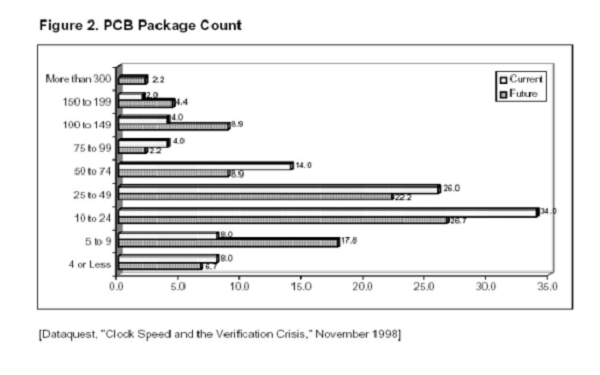
The increase in the number of package pins will exacerbate the current problems in the small-size, high-density layout. Perhaps, for those designers who are designing more complex circuit boards, they are not surprised that the next design will take more time.
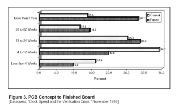
Although the market is clamoring to shorten the product design cycle, the reality is that the design of complex circuit boards actually takes longer, because designers must not only strive to obtain higher edge speeds, smaller sizes, and higher density packages. , Also consider issues such as signal integrity and timing. Since the layout is the main component of PCB design, it is clear that the high efficiency of these two processes will directly shorten the entire design cycle, while also improving overall productivity. The PCB market survey conducted by Printed Circuit Design Magazine in September 1998 concluded that: now there are more automatic operations for placement and routing tasks, and the design tools are not only automatic routing functions but also interactive. There were similar comments at this year's PCB design conference. Participants advocated one after another: The PCB field needs more easy-to-use layout tools.
During the transition period, a powerful and comprehensive PCB routing solution is needed. Not only can solve high-speed problems, meet the requirements of packaging and processing, but also must be automatic, interactive, comprehensive, and easy to use. Only in this way can the PCB design field be able to cope with the ever-increasing technical challenges well in the coming months and even years.
Still, need help? Contact Us: support@nextpcb.com
Need a PCB or PCBA quote? Quote now


 Surface

