
 NextPCB Capabilities
Printed Circuit Boards
NextPCB Capabilities
Printed Circuit Boards
 PCB Assembly
 Layer Buildup
 SMD-Stencils
 PCB Design-Aid & Layout
 Mechanics
 Quality
 Drills & Throughplating
 Factory & Certificate
 PCB Assembly Factory Show
Certificate
PCB Assembly Factory Show
Certificate
Support Team
Feedback:
support@nextpcb.com


This article is going to tell you about the PCB Copper Clad Advanced Connection Method on Altium Designer.
For example, the vias are fully connected, and the thermal pads are connected; the top GND network is fully connected, and the thermal pads of other layers are connected with a line width of 0.3mm.
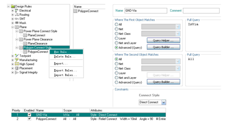
Step 1: In the AD PCB environment, Design>Rules>Plane> Polygon Connect style, click Polygon Connect style, right-click new rule, and create a new rule;
click the new rule to select the rule, and change the content in the name box. Modify the name of the rule, the default is PolygonConnect_1, now we modify it to GND-Via, choose Advanced (Query) for Where The Frist Object Matches, choose IsVia for Full Query (casing freely), choose Direct Connect for Connect Style, and other default settings. Click on the priority below to set the GND-Via rule priority to the highest, (1 is the highest, 2 is the second...) as shown in the figure below:
Step 2: Return to the PCB design environment for the copper pour, and choose GND for the copper pour network.
After the copper pour, the Via (via) where the network is GND will be a full copper connection instead of the default relief connect method (thermal pad method) ), since the rule is to pour the copper for the full connection of the via, the copper pour for the pad is a thermal pad connection method, as shown in the figure below (left):
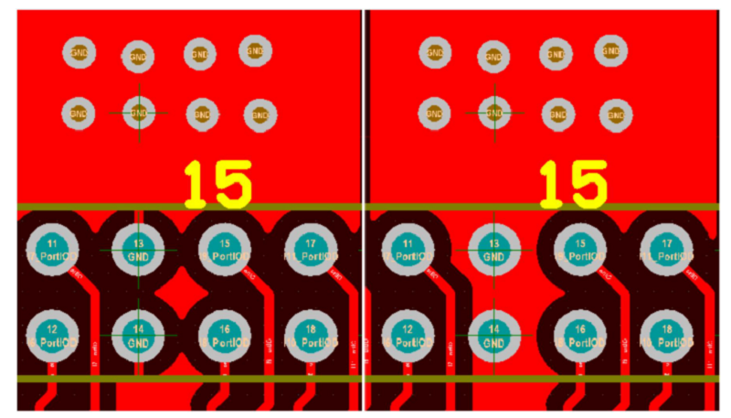
If you want to use thermal pads for vias and pads, change the Full Query to IsVia or Is pad, update the copper just now, and the ground pads are also fully connected, as shown in the picture above (right). The Full Query can also be Is pad, InNet('GND'), InNet('GND') And OnLayer('TopLayer'), InComponent('U1'),InComponent('U1') OR InComponent('U2') OR InComponent('U3' ), innetclass('Power') etc...
innetclass('Power'), the copper-clad connection method rule of Power class network, Design>Classes creates a ruling class, there are many kinds of class methods, such as network class, component class, layer class, etc. The network class points to the network name in the PCB, the layer class points to the component (welding position) in the PCB, and the layer class points to the layer in the PCB; Example: innetclass('Power'), create a new one under net classes The new rule is also added by right-clicking and renamed to Power. Select this network type rule and add the network on the left to the right, such as adding GND, VCCINT, VCC3.3, VCC1.2, VCCA, GNDA, etc... In this way, there is no need to separately establish GND, VCCINT, VCC3.3, VCC1.2, VCCA, GNDA copper-clad connection rules for different copper pours in multiple networks. You need to establish a network-type copper-clad connection rule. When copper-clad, the copper-clad network can be connected to the corresponding network;
Note: For all the above rules, you need to set the corresponding priority and create a new rule.
The priority of the new rule is set to high, the default rule has the lowest priority, and the other priority depends on the actual arrangement. For all options, select Where The Frist Object Matches and Advanced (Query), and Full Query to enter the corresponding data command. For the relatively simple ones, only the copper connection of the network and the layer InNet('GND') And OnLayer('TopLayer')-- -For the copper-clad connection method of the top-level ground network, you can choose The Frist Object Matches---Net and Layer, and then select the corresponding Net and Layer in the drop-down box inside. The software will fill in the data in the Full Query box, and then Apply OK and return to the PCB after completion (the syntax error in the Full Query box, the software will prompt an error, but filling in a non-existent layer or network name will not), and then proceed on the PCB For copper pour, select the corresponding copper pour network. The default copper pours pitch is 10mil. If you need a special pitch, you need to modify the pitch rules;
Still, need help? Contact Us: support@nextpcb.com
Need a PCB or PCBA quote? Quote now


 Surface

