
 NextPCB Capabilities
Printed Circuit Boards
NextPCB Capabilities
Printed Circuit Boards
 PCB Assembly
 Layer Buildup
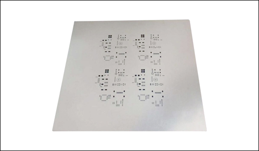
 SMD-Stencils
 PCB Design-Aid & Layout
 Mechanics
 Quality
 Drills & Throughplating
 Factory & Certificate
 PCB Assembly Factory Show
Certificate
PCB Assembly Factory Show
Certificate
Support Team
Feedback:
support@nextpcb.com


Filling up the stencil aperture with solder paste calls for a steel squeegee blade completing the solder paste right into the aperture. The alignment of the aperture relative to the squeegee blade influences the filling procedure. For example, apertures oriented with their brief axis towards the blade stroke load far better contrasted to those with their lengthy axis oriented to the blade stroke. Furthermore, as squeegee rate affects aperture fill, reduced squeegee rates attain far better loads for apertures with their lengthy axes oriented alongside the stroke of the squeegee.
The side of the squeegee blade additionally affects the method the paste loads the aperture of a stencil. The usual practice is to publish using minimal squeegee stress while preserving a tidy wipe of the solder paste on the stencil surface area. Raising the squeegee stress might harm both the squeegee blade and also the stencil, while likewise creating paste smearing listed below the stencil surface area.
The surface area place setting up procedure makes use of a stencil as an entrance to an exact and also repeatable solder paste deposition. A stencil is a slim sheet of aluminum foil of brass or stainless steel with a circuit stencil cut into it, matching the positional stencil of surface area install gadgets (SMD) on the published motherboard (PCB) for which the stencil is to be utilized. After precisely placing and also matching the stencil over the PCB, a steel squeegee pressures solder paste via the apertures of the stencil to develop down payments on the PCB for holding SMDs in position. The solder pastedown payments, when gone through the reflow stove, thaw and also safeguard the SMDs to the PCB.
The style of the stencil, particularly it's make-up as well as density as well as the sizes and shape of its apertures, figures out the dimension, form, and also positioning of the solder pastedown payments as well as this is essential to making sure a high-yield setting up procedure. As an example, the aluminum foil density, as well as the aperture opening dimension, specify the quantity of paste transferred on the board. An extra solder paste creates balling, linking, as well as tomb-stoning. Reduced quantities of solder paste reason completely dry solder joints. Both concession the electric capability of the board.
The kinds of SMDs on the board specify the optimal aluminum foil density. As an example, element bundles such as 0603 or SOICs with a 0.020" pitch need instead slim solder paste stencils, whereas a thicker stencil is preferable for parts such as 1206 or SOICs of 0.050" pitch. Although stencil density for solder pastes deposition varieties from 0.001" to 0.030", the common aluminum foil density that a bulk of boards make use of arrays from 0.004" to 0.007".
Today, the market utilizes 5 modern technologies for making stencils-- laser-cut, electroformed, chemically engraved, and also crossbreed. While crossbreed innovation is a mix of chemical etching as well as laser-cutting, chemical etching is extremely valuable for making action stencils as well as crossbreed stencils.
Chemical milling engraves steel masks and also versatile steel mask stencils from both sides. As this engraves not just in the upright instructions however likewise side to side, it creates damaging, and also makes the openings larger than preferred. As the etching follows 2 sides, the tapering on the straight wall surface creates the development of a shapely form, bring about additional down payments of solder.
As engraving the stencil openings does not generate a smooth outcome, the market makes use of 2 approaches for smoothing the wall surfaces. Among them is electropolishing, a micro etching procedure, and also the various other is nickel plating.
Although a smooth or refined surface area aids paste launch, it might additionally trigger the paste to miss the surface area of the stencil as opposed to rolling with the squeegee. Stencil producers resolve this trouble by brightening the aperture wall surfaces uniquely, however not the stencil surface area. While nickel plating enhances the stencil level of smoothness and also the printing efficiency, it lowers the aperture opening, which calls for artwork modification.
Laser cutting is a subtractive procedure, where Gerber information is fed to a CNC maker that regulates the laser beam of light. The laser light beam begins inside the limit of the aperture as well as goes across to its border, while totally eliminating the steel to create the apertures, one aperture at once.
Numerous specifications specify the level of smoothness of the laser cut. This consists of reducing rate, light beam place dimension, laser power, and also beam of light emphasis. Usually, the sector utilizes a beam of the light place of 1.25 mils, which reduces very accurate aperture dimensions over a large range of sizes and shape needs. Nevertheless, laser-reduced apertures additionally call for post-processing therapies equally as chemically engraved apertures do. Laser-reduced stencils call for electropolishing as well as nickel plating to smooth the within wall surfaces of the aperture. As the aperture dimension minimizes throughout the last procedure, the laser cut aperture dimension should be accordingly made up.
Publishing with a stencil entails 3 unique procedures. The very first is the aperture-fill procedure where the solder paste fills up the aperture. The 2nd is the paste transfer procedure, where the paste collected in the aperture transfers to the PCB surface area, as well as the 3rd is the positional place of the transferred paste. The 3 procedures are important to attaining the preferred outcome-- transferring a specific quantity of solder paste (additionally called a block) to the appropriate area on the PCB.
Still, need help? Contact Us: support@nextpcb.com
Need a PCB or PCBA quote? Quote now


 Surface


grenda
Nice page! Thank you for sharing.
kiewi
Stenciling is a decorative finish technique used to produce and exactly replicate a design or pattern.