
 NextPCB Capabilities
Printed Circuit Boards
NextPCB Capabilities
Printed Circuit Boards
 PCB Assembly
 Layer Buildup
 SMD-Stencils
 PCB Design-Aid & Layout
 Mechanics
 Quality
 Drills & Throughplating
 Factory & Certificate
 PCB Assembly Factory Show
Certificate
PCB Assembly Factory Show
Certificate
Support Team
Feedback:
support@nextpcb.com


A PCB is not just a structure designed to keep electronic components fixed and anchored. Its functionalities are deeper and embrace several criteria. An interesting journey to discover printed circuits.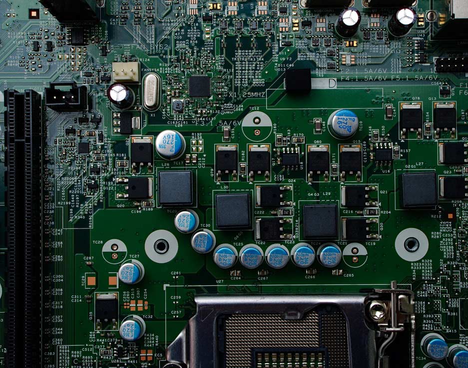
The designers of 40 years ago were real heroes. They did not have computers or software for designing printed circuit boards. However, they made high-quality PCBs, even for very complex designs and schematics.
Obviously, at that time, there were no circuits and high-frequency needs of our day. The manufactured products, both single-sided PCBs and double-sided PCBs, were able to satisfy most of the needs of customers, even the most sophisticated.
Today the speech is completely different. The high quality and performance of the electronic devices, the high frequency, the miniaturization, and the very high number of components mean that the final result must be extremely sophisticated.
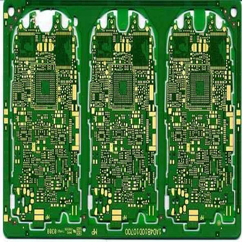
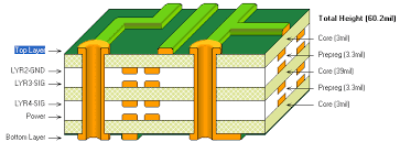
PCB design and creation of new PCBs involves professional factory construction, thanks to the use of specialized machinery. It is unthinkable, in fact, to manually create complex printed circuits consisting of 4, 6, or 8 layers. Consider, for example, the high technology contained in the latest models of computer motherboards.
There are different types of PCBs, depending on the applications required. Among the most widespread and important are those with:
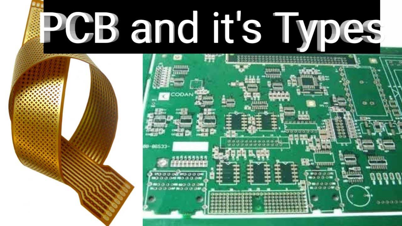
- single layer pcb
- double layer pcb
- multilayer pcb
- Flexible pcb
- with aluminum support, etc.
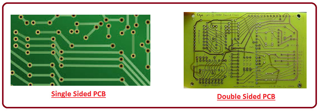
The simplest and cheapest type is obviously the single-layer one. The double-layer (or double-sided) PCB is already considerably more complex and able to solve several problems. It is composed of two thin layers of conductor around an insulating material.
The pads (linked together) must match perfectly on the two levels. The Multilayer PCB consists of at least three layers of conductive material. This type allows very complex realizations, allowing extremely compact assembly. Flexible PCBs use a pliable plastic material and can contain even multiple layers. It is used in various fields of application.
Electronic circuits are very different. PCBs differ from each other in operating frequencies, operating speeds, current powers, for use in the automotive or domestic sector, for medical applications, and more. This first distinction is already sufficient to understand the need for a different implementation approach.
Depending on the final use of the device, analysts will have to evaluate differently the design criteria of a PCB. Circuits need to be examined based on different practical and technical scenarios.
The volume of requests and the reduction in waiting times are also increasingly changing the PCB production market. Today the production method of printed circuit boards is extremely complex.
Due to the very small dimensions of the various elements (for example traces and holes), the working systems are supported by equally sophisticated instrumentation:
- microscopes
- X-rays
- HR scanners for checking Gerber files
- metallographic processes
- lasers, etc.
All the design phases are followed by computers and programmed machinery. The final quality is not dictated only by the customer's needs but must also be subjected to the most stringent conformity controls to obtain certifications.
Single-sided boards still make up a significant proportion of the world's printed circuit boards. In the previous decade in the United States, they accounted for about 70% of the volume of production of boards in quantitative terms, however, only about 10% in value. In the UK, these boards account for about a quarter of all production.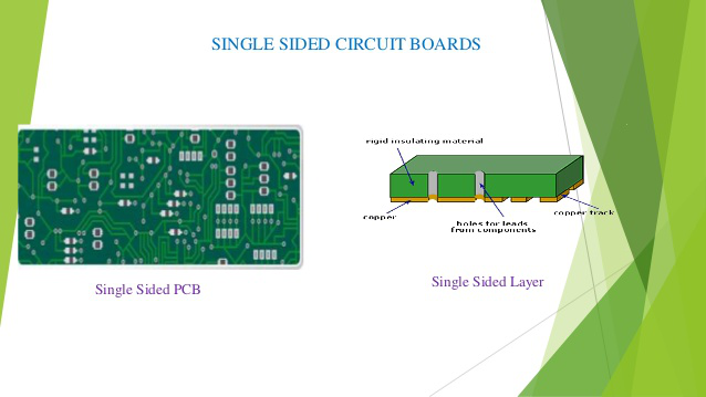
The route of manufacturing single-sided boards traditionally includes drilling, photolithography, etching of copper foil, surface protection and preparation for soldering, and separation of workpieces. The cost of single-sided boards is 0.1 - 0.2 of the cost of double-sided boards, which makes them quite competitive, especially in the field of consumer electronics.
Note, however, that for modern electronic devices, even for household use, single-sided boards often require contour milling, the application of protective masking coatings, and their assembly is carried out with the crystals being placed directly on the board or by surface mounting.
Double-sided boards currently account for a significant share of board output, for example in the UK up to 47%. Without pretending to be unambiguous, but relying only on our own statistics of the last three years, we can estimate the share of double-sided boards in Russian production at 65 - 75%.
Such significant attention of developers to this type of motherboard is explained by a kind of compromise between their relatively low cost and rather high capabilities.
The manufacturing process for double-sided boards, as well as single-sided ones, is part of the more general manufacturing process for Multilayer PCBs. However, for double-sided boards, pressing of layers is not required, it is much easier to clean the holes after drilling.
At the same time, for the majority of double-sided boards abroad, the "conductor / gap" design norms are 0.25 / 0.25 mm (40% of the output volume), 0.2 / 0.2 mm (18%) and 0.15 / 0.15 mm (18%).
This makes it possible to use such boards for the manufacture of a wide range of modern products; they are quite suitable for both through-hole and surface mounting.
The use of flexible dielectric materials for the manufacture of PCBs provides both the designer and the user of electronic devices with a number of unique possibilities. This is, first of all, a reduction in the size and weight of the structure, an increase in assembly efficiency, an increase in electrical characteristics, heat transfer, and overall reliability.
If we take into account the main property of such boards - dynamic flexibility - it becomes clear that the increasing scope of application of such boards in automobiles, household appliances, medicine, defense, and aerospace engineering, computers, industrial control systems, and on-board systems becomes clear.
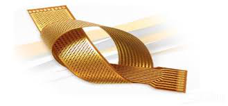
Flexible Printed Circuit Boards (FPC) is manufactured on polyimide or Mylar film. Therefore, it can easily deform even after the formation of a conductive pattern. Most flexible PCB designs are similar to rigid PCB designs.
Single-sided PCBs are the most common in this class of boards as they exhibit the best dynamic flexibility. The contact pads of such boards are located on one side; copper is most often used as a conductive foil material.
Rigid-flex PCB is hybrid designs and contains both rigid and flexible bases, fastened together into a single assembly and electrically connected by plated holes. They are most common in defense equipment, but their application is also expanding in industrial electronics.

A feature of the modern production of electronic devices is the increasingly widespread use of large and very large integrated circuits (LSI and VLSI). At the same time, the number of terminals of each circuit increases significantly, the distance between the terminals decreases from 2.5 mm to 0.625 mm or less.
Installation of multi-pin LSI and VLSI enclosures on printed circuit boards is technically and economically more efficient not in through holes, but on contact pads located on the surface of printed circuit boards.
This explains the increasingly widespread transition from mounting components in holes (PTH - Plated Through Hole) to surface mounting technology (SMT - Surface Mount Technology).
At the same time, at present, in most serial electronic blocks, both surface mounting and mounting through-holes are used.
This is because some of the components are not suitable for surface mounting. Besides, in devices operating in conditions of shock and vibration overloads, mounting through holes is preferred because of the more reliable fastening of components.
The process of assembling elements on the RP does not differ significantly from the standard processes. Mounting in holes and on the surface is possible using manual soldering, wave soldering, infrared and convection oven soldering. The only thing that needs to be taken into account when forming and installing elements is that the mounting lamellas are recessed by 0.1 mm relative to the board surface.
The board itself is an insulating and inelastic material. (There are also flexible PCBs) The thin connections seen on the surface of the board are Part of the conductive foil that covers the entire board at the beginning of the production phase.
This conductive foil is partially etched and the remaining copper paths form a network. These paths are called the Conductor Pattern and provide the electrical connection between the electronic parts mounted on the PCB.
It is the mask that gives PCB's green, blue, red, or brown color. This mask is an insulating and protective layer that protects the thin copper paths and prevents solder from touching anything other than the connection points of components.
Serigraphy is printed on the solder mask. This is the printing of text and symbols on the PCB, indicating the locations of the different components to be assembled. It may also be called a legend.
The printing quality of copiers and laser printers is very good. However, they can print on thin materials such as paper, tracing paper, and acetate. As these devices cannot print directly on the copper plate, the transfer material is used.
The circuit diagram is printed on transfer paper, heated, and transferred onto a copper plate. In this method, the function of the transfer material is to hold the powder paint (toner) and transfer it to the copper plate when it is heated.
Let us briefly explain the heat transfer method in terms of substances.
The printed circuit diagram is prepared using a drawing program. Since the transfer paper will be folded and taped on the copper plate, guidelines are placed approximately 1 cm or 0.4 inches outside the circuit boundaries in the drawing.
After printing on a blank paper, the transfer material is taped between the guidelines and printed again. In the proposed method, the lines between the guidelines are covered with duct tape.
After the copper plate is cleaned, the transfer material is folded and adhered to on the plate. The plate is ironed at the highest temperature (3rd stage) without steam for 3 - 5 minutes.
After the copper plate is allowed to cool for a few minutes in water, the bands are removed and the transfer material is slowly separated from the plate. Coated paper dissolves in water during this process. Printed circuit paths are formed by melting the plate in acid.
Before exploring the PCI manufacturing process, it is important to make it clear that the steps described in this article may vary between manufacturers. Each company has its procedures stipulated according to its structure and work method. We intended to show how printed circuit boards are produced generically.
With the PCI project duly revised, the first manufacturing procedure itself is drilling. Grouped in large panels, several fibrous plates (which will form the layers of the PCI) are perforated by large machines - some of which are capable of exceeding up to six panels at the same time.
A thin sheet of aluminum foil can be placed on the panels to absorb and aid in the distribution of the heat caused by the perforation, avoiding possible damage to the plate. The number of drills used by machines can vary, but in general, they have cartridges with 120 drills.
After removing the aluminum foil, the panels are cleaned. In this stage of the process, the plates pass away from contact with electrical currents, being restricted to contact with chemical substances. The substances used are chosen according to the material of the plates and metallic films.
Then, the PCIs still grouped go-to containers full of copper. Thus, the entire area of the plates, including inside the holes opened in the drilling, will receive a very thin layer of this metal.
The next step is the application of a photoresist film, a light-sensitive material that aims to create a coating to protect the copper layer of the PCIs from the action of UV rays, avoiding possible oxidation and short circuits.
This is a step that requires great care. The storage environments of the panels with the exposed photoresist film must be very hygienic so that foreign particles (such as dust) do not come into contact with the conduction areas of the plates.
Subsequently, the panels receive a film that will determine the layout of the “tracks” that will conduct the electrical current through the PCI. This new layer acts as a mask. It covers the parts of the surface of the plates that should not receive current.
The printed circuit boards go on to receive reinforcement in the copper layer in the parts that remain exposed, the “trails” and the holes from the drilling. The applications of the metallic substance are very thin, being thousandths of an inch thick.
Another metallic element comes into play: tin. This substance is added to the points where the areas recently bathed in copper are still exposed. It will serve as a protection for the contacts where the electronic components will be welded in the future.
Then, the PCIs proceed to the procedure of removing the photoresist film. The films are removed with machines, as the precision must be perfect so as not to affect other layers of the plates. Then, the panels are dipped in tanks with chemical components to remove the tin. At that moment, the structure that will be responsible for conducting the electric current is finished.
The plates go into the process in which they will receive the so-called welding mask, a type of varnish consisting of polymers that give a coating capable of permanently protecting the copper traces of the PCIs. Finally, the plates take on the green color that we know.
The panels are exposed to UV lights so that the welding mask dries and they can be manipulated. The excess varnish is removed and the plates go to a greenhouse or oven to cure them at high temperatures.
The manufacturing process begins its final phase. The printed circuit boards go to a device that can be understood as a giant printer, on which they will have the screen printed (such as the product name, version, indications of the positions of the components, and other information that will be useful in the assembly of the electronic components. ). Again, the PCIs are left to rest in a greenhouse or oven to dry the screen printing.
Finally, the plates are bathed in a welding flux - a substance that facilitates the welding procedure. The flux adheres only to the surface where the copper is still exposed. With the excess of this element removed, the panels can proceed to the final quality inspection.
It is not only at the end of the production process that the plates are checked. Visual inspections, when the human being ascertains imperfections in the plates, can happen at different moments of the line, varying according to the manufacturer.
Normally, in addition to the last superficial check, at the end of the production, the PCIs pass through machines that will test if the electric current is passing through the points specified in the initial project. That done, the printed circuit boards can now be separated or shipped in panels for customers - who will insert the electronic components that will make up the gadgets.
The thickness of a standard PCB board is 0.0629 inches or approximately 1.60 mm. There is a nominal tolerance in this thickness that has a limit of + or - 0.13mm, but in the vast majority of cases, the variations verified in practice are much smaller than this nominal tolerance.
This thickness, in addition to meeting physical and mechanical needs, in the vast majority of cases also brings great efficiency in terms of insulation and dielectric strength.
There are several thicknesses of materials available on the market, mainly in fiberglass (FR-4), in the case of Phenolate (FR-1 or FR-2) or Composite (CEM-01) the mechanical factors often make the use impossible of smaller thicknesses.
Damaged by the absorption of moisture and its own composition, phenolate undergoes warping tendencies and greater rupture facility as the thickness is reduced. In addition, other variations due to thermal dissipation and dielectric strength also worsen the performance of thinner plates.
That is why it is not so common to find phenolate slabs with thicknesses below 1.60mm on the market. Even so, there is the commercial availability of thicknesses of 1.20mm, 1.00mm, and 0.80mm.
The thickness of the copper that is pressed to the laminate also varies. When it comes to single-sided printed circuits, it is possible to state that more than 99% of the circuits are manufactured with 1Oz (one ounce) copper, which is equivalent to approximately 35 microns.
In specific cases, different thicknesses are used, mainly in circuits with high current points, it is necessary to use 2Oz copper (two ounces) or even more.
Due to the much higher cost of two-ounce copper laminates, it is very common that in generations of the board design, designers try to thicken the tracks that lead to higher currents as much as possible and often choose not to protect these trails with the anti-welding mask so that it is possible to reinforce this trail with the application of tin on it during the assembly process.
The different nature of the devices also dictates the requirements for the choice of materials. Depending on the application, in fact, the different types of substrate can affect the final results differently. It is not possible to create an ideal or perfect printed circuit as each electronic board performs a unique type of work, according to the electrical needs and the required performance.
Still, need help? Contact Us: support@nextpcb.com
Need a PCB or PCBA quote? Quote now


 Surface

