
Support Team
Feedback:
support@nextpcb.comWith the development of micro-device manufacturing and surface mounting technology, the width of the PCB trace becomes narrower and the space between traces becomes smaller, promoting the rapid progress of fine line manufacturing technology.
As a leading PCB manufacturer, NextPCB has been committed to providing customers with the most advanced and cutting-edge manufacturing technology. NextPCB adopts LDI exposure technology in the image conversion process during PCB fabrication. The minimum line width that NextPCB provides is 3.3mils, which is far ahead in the PCB industry. This article analyzes the differences between LDI exposure and traditional CCD exposure techniques
.
The definition of LDI
LDI, the full name is laser direct imaging. It is a technology that UV Light or laser light is used to transfer the image required by the customer to dry film on the substrate. Then the dry film undergoes polymerization and cross-linking reaction, making the image transfer to the board surface. Finally, the customer’s desired image is formed with some post processes.
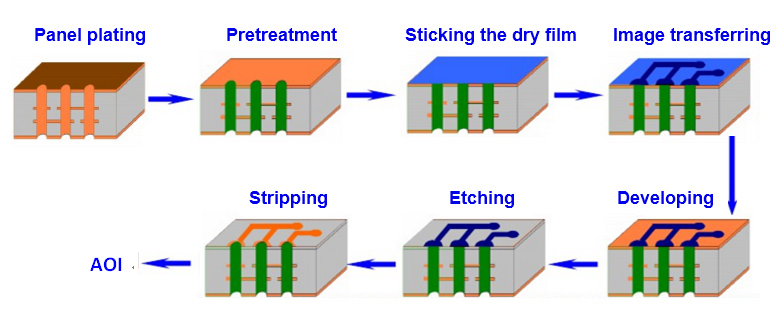
The procedure of LDI
The differences between LDI and traditional CCD exposure technology
> The comparison of imaging methods LDI: laser direct imaging
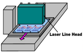
Printing the image on the dry film directly
> Traditional exposure machine imaging
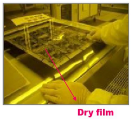
UV light is used to transfer the fixed pattern from the film o the dry film
Through the comparison, we know that the apparent characteristic of LDI is that LDI provides an image directly without using a film. The use of traditional film may cause lots of problems such as poor dimensional stability, easy to deformation and elongation. And due to the limited number of uses of the film, it is time-consuming to replace the film and adjust the alignment regularly during the operation. In the actual production, it is quite common to replace 30 to 40 sets of films in a 20 hours’ operation. The total time is 300 min to 400 min if each replacement takes 10 mins, which is equivalent to consuming 5h-6.5h of a working day. But in the LDI system, the line replacement usually takes only a few seconds.
> The comparison of alignment ability
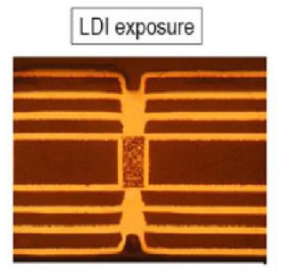
LDI: direct imaging exposure
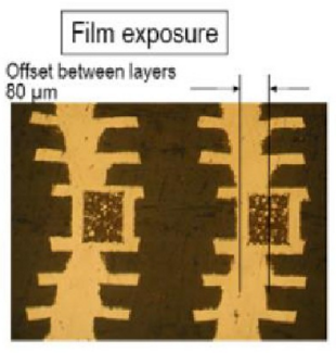
Traditional exposure machine imaging
By comparing the differences in alignment capabilities, it is obvious that the LDI system has a higher position accuracy. And the LDI system has greater advantages and better quality in the high-density PCBs and the multilayered PCBs with buried/ blind vias.
The analysis of LDI resolution capability and inner layer AB differences
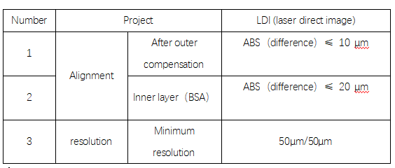

Resolution: 50μm/50μm Good analytical Inner layer AB difference ≤ 20 μm
> The LDI capability of NextPCB
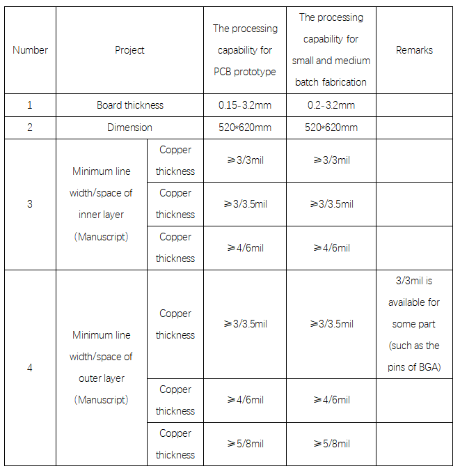
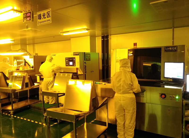
LDI technology not only improves imaging stability but also effectively controls the cost and improves the manufacturing efficiency. As a professional PCB assembly manufacturer, each process during manufacturing is equipped with high-end machines. And all the processes are strictly quality controlled. Our manufacturing capability can meet the different demands of different customers.
Still, need help? Contact Us: support@nextpcb.com
Need a PCB or PCBA quote? Quote now