
 NextPCB Capabilities
Printed Circuit Boards
NextPCB Capabilities
Printed Circuit Boards
 PCB Assembly
 Layer Buildup
 SMD-Stencils
 PCB Design-Aid & Layout
 Mechanics
 Quality
 Drills & Throughplating
 Factory & Certificate
 PCB Assembly Factory Show
Certificate
PCB Assembly Factory Show
Certificate
Support Team
Feedback:
support@nextpcb.com


Designing a circuit board, or a Printed Circuit Board (PCB), is a complex task that requires an understanding of electrical engineering, components, software tools and manufacturing. It can be a daunting task for new designers looking to design their first PCB board. In this article, we look at the basic steps involved in creating a circuit board and some considerations designers need to take into account to minimize errors.
The first step in designing a circuit board is schematic capture. This is the process of creating a diagram of the circuit using a software tool. The diagram shows the components and their interconnections. At this stage, designers may use simulation tools to test the outputs of the circuit under different inputs and conditions.
The next step involves finding the footprints of all the parts, positioning them on PCB board and drawing or routing the traces between the pins.
This stage requires designers to take into account many design considerations such as the spacing between components, trace widths, and overall board size and their influence on manufacturing and cost. The routing process involves selecting the appropriate trace width, spacing, and layer configuration to ensure that the circuit functions correctly and meets any design requirements.
Electrically, component placement and routing can impact noise, interference, and heat dissipation. From a manufacturing standpoint, designers must ensure that their chosen fab house can manufacture their design and that their design falls within their manufacturing specifications and tolerances. Designing a board with unnecessarily tight spacings could increase costs when they could be avoided.
Inadequate component spacing can cause interference effects or make manufacturing defects more likely
Once component placement and routing are complete, some EDA software have built-in DRC checks which checks against a set of rules to ensure that it meets any design requirements and manufacturing constraints set by the user.
Some common design requirements that can be checked during the DRC process include:
The width of the conductive traces on the PCB is important to ensure that the circuit functions correctly. The DRC process checks that the trace widths are within the specified limits.
Clearance refers to the distance between different components or traces on the PCB. The DRC process checks that the clearance is sufficient to prevent electrical interference or short circuits.
The spacing between the pads of different components is important to ensure that the components can be mounted correctly and that the circuit functions correctly. The DRC process checks that the pad-to-pad spacing is within the specified limits.
The size of the holes on the PCB is important to ensure that the components can be mounted correctly and that the vias can carry the required current. The DRC process checks that the hole sizes are within the specified limits.
The layer stackup refers to the number and arrangement of the layers in the PCB. The DRC process checks that the layer stackup is appropriate for the design requirements and manufacturing constraints.
The mask and silkscreen layers on the PCB are used to indicate solder mask openings and any areas of silkscreen printing required.
Once the design has been verified, The final step is to generate the Gerber files, which are used to manufacture the PCB. Every PCB design software translates the design into Gerber format in a different way, which may not be compatible with your chosen manufacturer. This is why it is important to use a Gerber Viewer to view the data and check with your manufacturer to ensure your design is communicated correctly.
HQDFM Gerber Viewer is an advanced online Gerber Viewer from NextPCB that is free to use and does not require sign-up. It also has an integrated DFM tool to check for manufacturability issues with most factories.
After verifying your production files, they can be sent off to your chosen manufacturer for fabrication. PCB manufacturers like NextPCB can also handle components procurement and assembly for you, which both saves you time and ensures the boards are built to industrial quality standards. For this, you will require additional files including the BOM and centroid data (pick and place file).
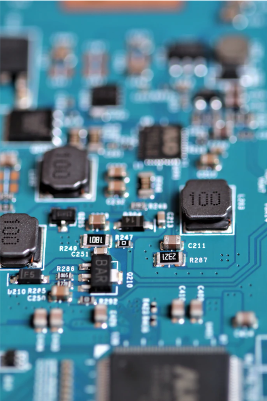
Once the PCBs and components are ready, soldering can begin. This can be done by hand or consigned to assembly houses for larger and more complex designs.
After the boards are assembled, they should be tested to ensure they function as expected.
Complex designs with tiny components are more suited for machine assembly
The goal of PCB design is to create functional, reliable, cost-effective circuit boards that meet the electrical and physical requirements of the devices they will be used in. PCB design is also critical to make sure devices function properly and minimize the risks of electrical shorts, interference, and other problems that can arise with poorly designed circuits.
There are many PCB layout software options available, each with its own strengths and weaknesses. Here are some popular options:
An open-source PCB design tool that is free to use. It has schematic capture and PCB layout modules with good feature sets.
A low-cost but powerful PCB design tool that is popular among hobbyists and professionals. The free version has size restrictions.
A professional-grade PCB design tool with advanced features. It's expensive but industry standard for complex designs.
A suite of PCB design tools by Cadence with everything needed for circuit design and integration.
An affordable PCB design tool with great usability. Has versions for different complexity needs.
A free online circuit design and PCB layout tool with library parts and design sharing.
An open-source software focused on electronics learning and rapid prototyping.
Provides co-simulation by combining PCB layout with microcontroller simulation.
Multisim by National Instruments focuses on circuit simulation but also integrates PCB layout.
Many of these provide free versions with limitations that are great for beginners learning PCB design. As needs grow, paid versions provide more advanced capabilities.
HQ NextPCB is a Chinese-based PCB manufacturer and assembly with an emphasis on reliability. NextPCB's capabilities include up to 32 layer boards, blind and buried vias up to HDI 3, custom stack-ups, full turnkey assembly and more via a smart quotation platform with dedicated one-to-one support. HQ NextPCB can also be used with HQ Online, a collection of over 300,000 parts including connectors, passives and ICs for super-fast PCB assembly. Try them for your next design at HQ NextPCB.com and see the difference.
Still, need help? Contact Us: support@nextpcb.com
Need a PCB or PCBA quote? Quote now


 Surface

