
 Surface


Zhang

 NextPCB Capabilities
Printed Circuit Boards
NextPCB Capabilities
Printed Circuit Boards
 PCB Assembly
 Layer Buildup
 SMD-Stencils
 PCB Design-Aid & Layout
 Mechanics
 Quality
 Drills & Throughplating
 Factory & Certificate
 PCB Assembly Factory Show
Certificate
PCB Assembly Factory Show
Certificate
Support Team
Feedback:
support@nextpcb.com


In the PCB manufacturing and assembly (PCBA) process, Panelization is the critical "last mile" that connects design blueprints to mass production success. For Rigid PCBs, an excellent panel design not only ensures the stability of SMT placement but also directly saves thousands of dollars in manufacturing costs by improving material utilization.
This article provides an in-depth analysis of rigid PCB panelization strategies, design specifications, and how to avoid common DFM (Design for Manufacturability) pitfalls.
Panelization involves arranging multiple smaller PCB units onto a larger substrate, making it a unified entity that is easy for automated machinery to handle. For procurement managers and electronics engineers, its core value lies in:
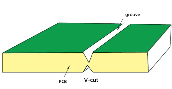
In rigid PCB design, there are two primary methods for separating boards. The choice depends on the board's shape and component layout.
This is the most common and cost-effective method. The manufacturer cuts V-shaped grooves on both sides of the board, leaving about 1/3 of the board thickness as a connection.
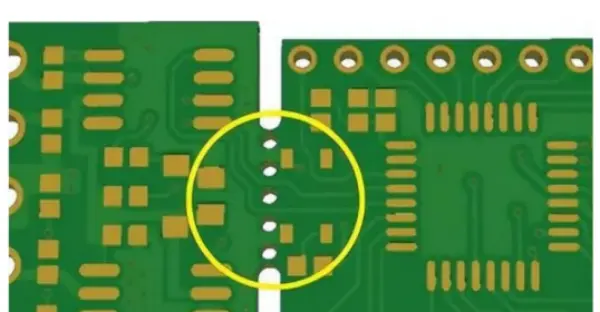
A router bit is used to mill out the board shape, leaving only a few connection points (tabs) with small holes (mouse bites) for easy breaking.
Engineer's Insight: For complex hybrid designs, the panelization strategy changes drastically. For instance, in Rigid-Flex PCB design, flexible materials cannot withstand the pulling force of V-scoring, so laser cutting or special die-punching is often required. If you are weighing the manufacturing challenges of different PCB technologies, we recommend reading our in-depth guide: Flex vs Rigid vs Rigid-Flex PCB: Which is Better for Your Project?
To ensure your panel design passes NextPCB's CAM review and reaches mass production smoothly, follow these industry standards:
This is the most frequent cause of scrap. If fragile components (especially ceramic capacitors or crystals) are too close to the V-cut line or tabs, the stress of separation can cause micro-cracks.
Calculating spacing, confirming rails, and checking keep-out zones manually is time-consuming and prone to error. NextPCB's self-developed HQDFM software provides a smart solution to these challenges.
HQDFM is an intelligent software suite integrating DFM (Design for Manufacturability) and CAM engineering analysis, offering flexible solutions based on user needs:
Engineer's Recommendation: Use the Online version for initial checks. For complex projects heading into mass production, downloading the HQDFM Desktop Suite for a full DFM analysis is the best practice to ensure first-pass success.
One-Click Detection of Panelization Risks with HQDFM - All Free Try Lightweight Gerber Viewer Online
Many designers set panel sizes arbitrarily, leading to very low utilization of standard copper-clad laminates (sometimes as low as 50%).
| Capability Item | Specification / Value | Notes / Description |
|---|---|---|
| Panelization without space | 0 mm | Zero spacing between boards in the panel (used for V‑cut arrays) |
| Panelization with space | ≥ 1.6 mm | Minimum 1.6 mm gap recommended when routing (milling) between PCBs |
| Panelized round board | ≥ 80 mm × 80 mm | Suitable for round PCBs with stamp holes (≈0.5 mm hole Ø / 0.35 mm copper gap). Default uses ~5–7 holes per break tab for strength |
| Panelized castellated holes board | With stamp holes + tooling strips | Supports castellated‑hole boards with edge tooling strips; ensure distance from holes to corners per guidelines |
| Minimum width of breakaway tab | ≥ 4 mm (≥ 5 mm for mouse‑bites) | Breakaway tabs should be ≥4 mm; if using mouse‑bites, ≥5 mm is recommended to reduce cracking |
| Minimum edge rails | ≥ 3 mm | Edge rails provide mechanical support for SMT conveyors and reflow fixtures; default panels include ≥3 mm edge rails on long sides |
A well-designed rigid PCB panel is the cornerstone of efficient manufacturing. While V-scoring offers the best cost-benefit ratio for standard designs, tab-routing remains the go-to for irregular shapes. Utilizing digital tools like HQDFM significantly reduces the risk of design errors.
However, as products become smaller and more 3D-oriented, rigid PCBs alone may not meet every requirement. When your design involves 3D assembly or dynamic bending, understanding the fundamental differences in structure and panelization between rigid and rigid-flex boards becomes vital.
>> Explore more on choosing the right PCB technology: Flex vs Rigid vs Rigid-Flex PCB: A Technical and Application Comparison
NextPCB is committed to providing high-reliability PCB manufacturing and assembly services. Upload your Gerber files to HQDFM for a free check today, and our CAM engineers will provide professional panelization optimization suggestions.
PCB panelization is the process of arranging multiple board designs onto a larger panel for more efficient manufacturing and automated assembly. Good panelization includes board array layout, break lines (V‑score or tab routing), and fiducial/tooling holes.
Cracking or warping during board separation usually comes from poor scoring or routing design, or insufficient support during depanelization. Properly designed V‑scoring depth and tab spacing reduces mechanical stress.
Automated pick‑and‑place machines rely on fiducial marks and tooling holes for accurate alignment. Missing or poorly placed fiducials can cause misalignment or incorrect placement.
If components are too close to panel edges or scoring lines (< 3–5 mm), the mechanical forces used in depanelization can damage parts or solder joints. Always leave adequate clearance between components and panel edges.

Still, need help? Contact Us: support@nextpcb.com
Need a PCB or PCBA quote? Quote now


niidme
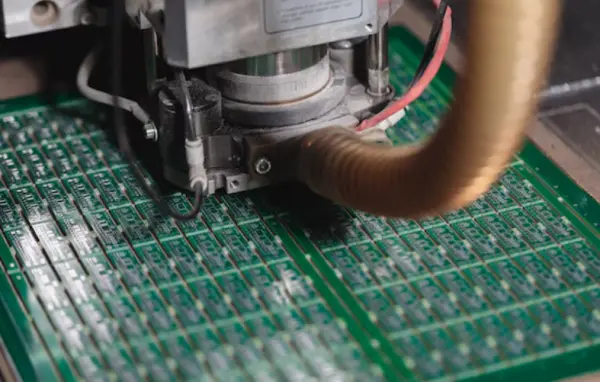
SMT process: Printing--> inspection--> placement - >Inspection ->Welding -->Inspection --> Maintenance--> board splitting