NextPCB Capabilities
Printed Circuit Boards
NextPCB Capabilities
Printed Circuit Boards
 PCB Assembly
 Layer Buildup
 SMD-Stencils
 PCB Design-Aid & Layout
 Mechanics
 Quality
 Drills & Throughplating
 Factory & Certificate
 PCB Assembly Factory Show
Certificate
PCB Assembly Factory Show
Certificate
Support Team
Feedback:
support@nextpcb.com


In the particular gigantic field of electronics, designing Printed Circuit Boards (PCB) has assumed an ever-increasing importance. The actual invention of the PCB dates back to February 1943 -PCBs have been around for a very long time and yet most of us still find designing them to be a difficult task. This article intends primarily to give a guide to young and experienced designers who are eager to acquaint themselves with efficient design principles of PCBs.

Always begin your PCB with a schematic. The schematic acts as a blueprint of what you are trying to create. It graphically represents the PCB’s components and the connections between them in a logical manner.
The road to a good schematic design entails:
Another important point to make is that, a circuit diagram is only a schematic drawing. What does this mean? It means that the circuit diagram should not be taken too literally. It only tells us where to make connections between components, but the order /positioning of the components is up to designer. Remember, the circuit diagram is not to be taken too literally.
The immediate step after studying and understanding the circuit diagram is to transfer it in to a drawing of your Printed Circuit Board (PCB). The layout of your circuit on the PCB will have a significant impact on its performance. Poor PCB layout can lead to functional and reliability issues.
Here are a few ideas that will help you create good designs.
A large number of different materials are available throughout the world, suitable for every application. Agree? The material selected to make up your PCB must:
|
|
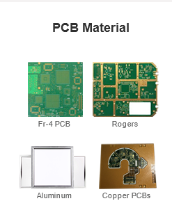
source: NextPCB
ESD protection must be included in a good PCB design. This measure is taken to avoid component/device failure caused by externally induced high-voltage level impulses, which can impact system operations. ESD effects range from noise and disturbance of measurement equipment to a complete component damage.
Below is a list of efficient design techniques for ESD protection
Because PCB documentation saves so many hours of design time, designers must be aware of documenting the correct information in the correct format in order to successfully manufacture their final product.
The numerous PCB documents a designer must have include a Bill of Material (BOM), PCB overlay Gerber File and many others. These documents must complete. The Gerber file should have defined apertures to avoid error and PCB production delay.
The above five tips serve as a guide to a PCB designer during the design process. After the PCB has been successfully designed, one can contact NextPCB PCB Prototype Assembly and Manufacturing for high quality PCB production.
|
|
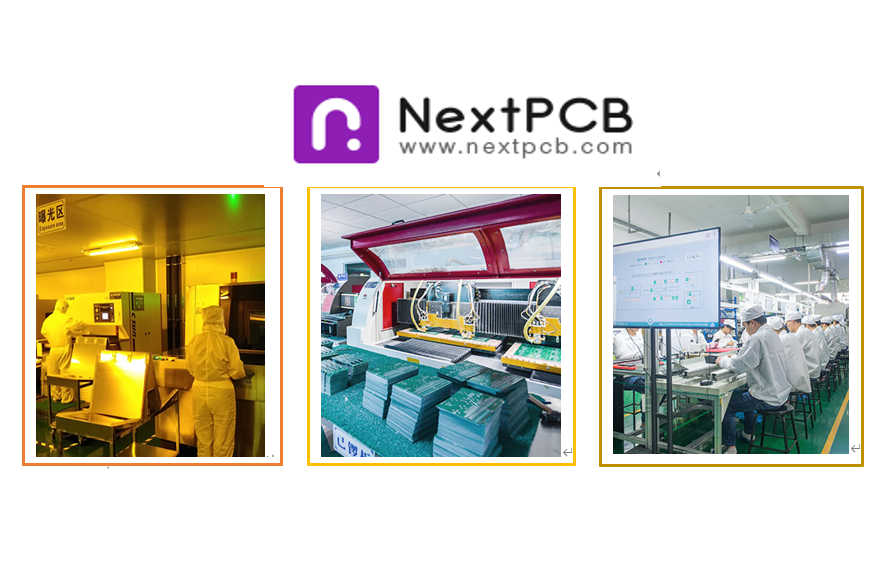 NextPCB is one of the most experienced PCB manufacturers in the world, with over 15 years of experience in the PCB and assembly industries. NextPCB can meet your requirements for PCB prototyping, small PCB production, and mass PCB production. It offers the most innovative printed circuit boards and assembly technologies in the highest quality standards, as well as the quickest delivery turnaround of up to 24 hours.
This company operates three factories specialising in PCB Prototype, PCB Mass Production, and PCB Assembly, all of which are equipped with AOI, X-Ray Testing, and Multiple Functional Testing.
It follows the customer-first principle. It assembles a professional team of salespeople, marketing specialists, and engineers, each of whom has more than five years of experience in the PCB industry.
Any questions don't hesitate to contact nextpcb .
Still, need help? Contact Us: support@nextpcb.com
Need a PCB or PCBA quote? Quote now


 Surface