Contact Us
Blog >> Blog Details Page

What’s the Difference Between PNP and NPN Transistors?

Posted:09:41 AM November 23, 2023 writer: The Engineering Knowledge

Introduction

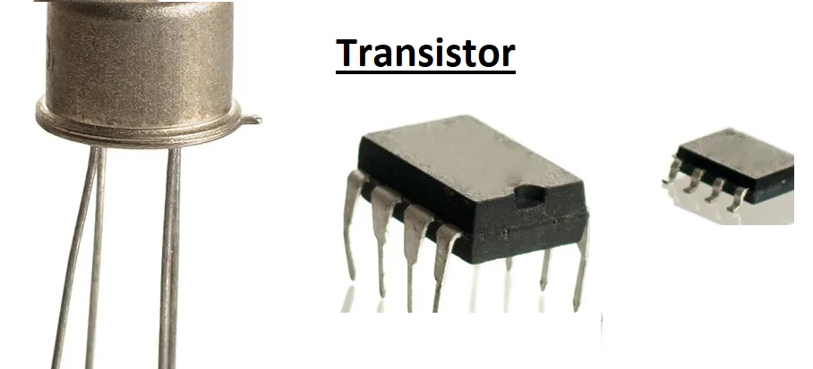
The transistor is a very common building block of electronic devices and circuits. Its commonly used type is BJT which is very common in electronic circuits. There are two types of BJT NPN and PNP transistors. These two types of transits will be covered in detail in this post and are basic components of switching and amplifier circuits.

Working of Transistor

The transistor operates as a signal switch, which means it operates like an electron gate to open and close in seconds many times. It makes sure the circuit is in an ON state when current passes through it. Transistor are employed in telecommunication system as switch to control functions of different devices. using transit circuits have high switching speeds of about hundreds of Ghz or in some cases 100 billion in one second on and off.

For the composition of different input curent to have different output values transistor can connected to make logic gates. In computer logic, gates are used to solve problems with the use of Boolean algebra. This feature helps to use different computer programs

Transistor Mode of Operation

Cutoff Mode

  • In cutoff mode, the transistor is in the off state. No current passes collector to emitter for NPN or from emitter to collector in PNP. It happens for zero volts across the base pin of NPN or in the case of PNP base volts are larger than emitter volts. In this operating mode, the transistor works like an open switch

Saturation mode

  • In this mode of operation, the transistor is in on state, helping the highest current flow from the collector to the emitter for NPN and for the PNP emitter to the collector. This condition is caused when the voltage at the base pin is connected in NPN and for PNP base volts are lower than emitter volts. Here transistor is like a closed switch allo current flow

Active Mode

  • In this mode, transistor operation is between the situation and cutoff mode. The transistor works as an amplifier for this mode. Small variations in base curent cause a high effect on collector current. The transistor is in active mode, which helps to amplify signals. Active mode is commonly used to amplify circuits

Get Free PCB Assembly

BJTs and FETs

What is BJT

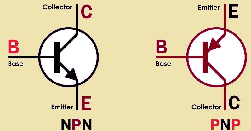
BJT full-form Bipolar junction transistor? BJT is made of three layers of semiconductor materials and it has two main types NPN or PNP. They are also known as negative positive negative and positive negative positive. The three layers of bjt are emitter, base, and collector. The emitter releases charge carriers electrons or holes in the transistor. The base is a control transistor that controls charge flow from the emitter and collector. While in collectors charges carriers of the base come.

The basic working of BJT is that the current provided at the base with a small value controls the current flowing between the emitter and collector. If the transistor is accurately biased charge carried moves from the emitter to the collector. BJT is part of the amplifier and digital circuits.

What is FET

The full form of FET is a field effect transistor. The function of FET is based on an electrical field instead of moving charges either electrons or holes as done in BJT. It has two main types. It also has three input sources, a gate, and a drain. At the source pin majority of carriers' energy comes out in FET. The gate is like a base that controls the charge flow between the source and the drain. Drains are also used for entry or existence of carriers.

N channel FET and P channel FET. In N channel FET the electroons are the majority charge carrier. Electron follow is regulated by an electrical field connected with a gate pin. While in the P channel majority of carries are holes. Hole flow is controlled with an electric field connected with a gate pin like an N channel.

FETs used in circuits due to their high input impedance make them best to use where high impedance is needed. So it is used on oscillators and amplifiers.

What is an NPN Transistor?

  • NPN is a type of BJT transistor used as a switch and amplifier. NPN defines the configuration of semiconductors in the transistor.
  • It has three layers, N, p, and N. In the N layer electrons are the majority of charges and it is known as an emitter.
  • P is a central layer that is sandwiched between two N layers and controls the electron flow.
  • The third N layer is collectors, collecting electrons from the emitter.

Operation of NPN Transistor

The operation of an NPN transistor is that the current flowing from the emitter to the collector is controlled by the small current of the base and emitter junction. Some details of the operation of the NPN transistor are explained here

Forward Biased condition

  • In this mode of operation, a small voltage is provided to the base-emitter junction in forward-biasing configuration. Due to this biasing electrons flow from N to the P region

Electron flow in Emitter

  • Due to this biasing state electrons in the N emitter have enough energy that helps to cross potential barriers and go in A type base

Base as Control

  • Current moving from the emitter to the base is less but it controls the larger curent flowing from emitter to collectors.

Base-Collector Junction

  • In this junction, there is a reversed biased condition avoiding a larger number of electrons from moving direct emitter to collectors

Current amplification

  • Small curent passes from emitter to base regulate high curent flow from emitter to collector.  This curent amplification is the main feature of the NPN transistor to use in electronic projects.

Electrons at Collectors

  • Electrons go to the base and then move to a collector in a reverse biasing state. At collectors, larger electrons are collected, and the end current in the transistor

What is a PNP Transistor

A PNP transistor is also part of switching and amplifiers. it has three layers and pins that are P, N between two P, and the third one is P. First P has holes are the majority and is known as an emitter. N is a base region that controls the current due to the hole. P is the collector terminal where holes from the emitter go.

Operation of PNP Transistor

The transistor is a current control electronic component that comes with two depletion layers having certain potential batteries for crossing depletion layers. In the case of silicon value of volts of potential barriers is 0.7 volts and for germinum is 0.3 volts. Silicon transistor is commonly used since it abundant element on earth.

PNP transistor structure is such that the collector and emitter are doped with P material of the periodic table and the base is a minority carrier of n material.  The emitter region is doped more highly than the collector region. its three regions make two actions base-emitter and collectors base junction.

If a negative voltage is provided across the base-emitter junction, electrons, and holes start to gather across the region. if the potential is less than 0.7 volts, barrier voltage comes, and diffusion starts. So electrons move to the opposite side and base curent in reverse side fo electron flow. If voltage is provided at the collector-emitter junction current flows from emitter to collectors. So PNPN transistor works amplifier and switches

Difference Between NPN and PNP Transistor

Characteristic

NPN Transistor

PNP Transistor

Semiconductor Type

it uses N semiconductor at collectors

It has a P semiconductor for the collector

Current Flow

Electrons move from emitter to collector

It has majority carriers holes flow from emitter to collectors

Biasing

At base positive voltage provided

it needed negative voltage at the base

Operation

electrons move from emitter to collector making N-type to P-type current flow

Holes flow from the emitter to the collector, forming a P-type to N-type current flow

Voltage Polarities

The collector voltage is higher positive than the emitter

The collector voltage is negative than the emitter

Applications

Amplifier and switch

Switch and amplifier

Example Use

digital logic circuits and amplifiers

digital logic circuits and amplifier circuits

Get Instant Online Quote

Applications of NPN and PNP Transistor

NPN Transistor Applications:

  • NPN is used for amplifiers in electronics. Its common emitter mode is used to work as an amplifier for weak signals
  • NPN is also used in Darlington pairs that have high curent gain. This circuit is used in applications where a high value of amplification is needed.
  • It is used in inverters that transform logic levels from high to low and low to high
  • it used is switch. if it is based in an active region curent flow from the collector to the emitter and works as a closed switch. In the cutoff, the region operates as an open switch, restricting current flow.
  • it is used to make oscillators that produce a continuous signal in sine, square shapes.
  • it used as an audio amplifier

PNP Transistor Applications

  • The uses of PNP are listed but some are like NPN
  • It is used as a signal amplifier like NPN but the difference is that it has a common emitter circuit.
  • it is also used as a switch, if it is biased in active region current flow from emitter to collectors, and works as a closed switch. It is an open switch for the cutoff region
  • it is also used in the Darlington transistor for high current gain.
  • it is used in inverters for the conversion of logic levels
  • it is used as a voltage regulator to stabilize and regulate voltage.
  • It is used in audio amplifiers as complementary to NPN

List of some common BJTs

Here you can see lists of some differnt types of BJTs. These are explained in their uses

  • NPN Transistors:
    • 2N3904
    • BC337
    • PN2222A
    • BC547
    • 2N2222
  • High-Frequency Transistors:
    • BF199 (NPN)
    • 2SA1145 (PNP)
    • BF180 (PNP)
    • 2SC3355 (NPN)
  • Power Transistors:
    • MJ15003
    • MJ2955
    • MJ15004
    • 2N3055
  • General-Purpose Transistors:
    • BC546 (NPN)
    • 2N3906 (PNP)
    • BC556 (PNP)
    • 2N3904 (NPN)
  • Low Noise Transistors:
    • 2SC2240 (NPN)
    • MPSA42 (PNP)
    • 2SA970 (PNP)
    • MPSH10 (NPN)
  • Audio Amplifier Transistors:
    • MPSA18
    • MPSA28
    • BC548
    • BC558
  • Switching Transistors:
    • 2N4401 (NPN)
    • S8550 (PNP)
    • 2N4403 (PNP)
    • S8050 (NPN)
  • Digital Transistors:
    • DTC114 (NPN)
    • MMBT3906 (PNP)
    • DTC144 (PNP)
    • MMBT3904 (NPN)

Transistor Advantages

  • it used to make single ICs
  • it is very low cost and comes in small size so easily connected in circuits
  • it makes high-efficiency circuits
  • it has low mechanical sensitivity
  • High-speed switching
  • it uses about zero power
  • Its operating life is longer
  • Cathode heaters have almost zero power consumption
  • its operation is safe since uses low-volts
  • It controls power to loads in inverters and choppers
  • it used in robots
  • it used in heavy motors for current flow
  • There is continuous power produced with the use of transistors in matched pair circuits

Disadvantages of transistor

  • it has less mobility of electrons
  • it is easily affected by cosmic rays.
  • it also damaged due to electrostatic discharge
  • it has a sensitive nature to temperature.
  • it generated low-energy
  • Power transistors do not operate well for a switching frequency of 15 kHz
  • its reverse blocking featues are low.
  • Second breakdown or thermal runaway damages the transistor
  • it needs clean condition and its construction is difficult
  • Its small size makes its tracing difficult in circuits when it is damaged. So  its unsoldering process is not easy

Conclusion

The differences between PNP and NPN transistor is very small like some letter and symbols but it has a very high impact on the functions of circuits where it is used.  NPN transistors have negative positive negative designs that work through current to flow from collectors and emitter. its base works as a control that controls the current flow from collector to emitter. While PNP comes with a positive-negative-positive configuration, works in the reverse state means curent flow from emitter to collectors. FET is also the type of transistor that has three pins like the BJT transistor. Its pins are the gate, drain, and source.  it uses an electrical field for curent flow control in semiconductors. Its two types of junction gate are FET and metal oxide semiconductor FET.

You may also be interested in...

What is P-type Semiconductor and N-type Semiconductor?

What's the difference between MOSFET and BJT and how to choose?

Autumn Offer: Get $30 off PCB orders over $100 with NextPCB

HQ NextPCB Introduces New PCB Gerber Viewer: HQDFM Online Lite Edition

  • PCB
    Prototype
  • PCB
    Assembly
  • SMD
    Stencil

Dimensions: (mm)

×

Quantity: (pcs)

5
5
10
15
20
25
30
40
50
75
100
120
150
200
250
300
350
400
450
500
600
700
800
900
1000
1500
2000
2500
3000
3500
4000
4500
5000
5500
6000
6500
7000
7500
8000
9000
10000

Other Quantities:(quantity*length*width is greater than 10㎡)

OK

Layers:

Thickness:

Quote now