Support Team
Feedback:
support@nextpcb.comIntroduction
The semiconductor industry has become an integral part of our modern lives, powering the devices we use every day. From smartphones and laptops to cars and home appliances, semiconductors play a crucial role in enabling the technology that surrounds us. But have you ever wondered how these tiny chips, also known as integrated circuits, are made? In this article, we will explore the fascinating process of manufacturing chips and wafers, which form the backbone of the semiconductor industry.
Making computer chips involves using a special material called silicon. Silicon is great for this job because it has unique properties. We get silicon from sand, and there's a process to make it super pure. Now, we take this pure wafer silicon and cut it into thin slices called wafers. Wafers are like the starting point for making chips. Next, we draw the circuit on the wafer using a process called photolithography. It's like making a blueprint for the chip. The smaller and more detailed the blueprint, the more powerful the chip can be.
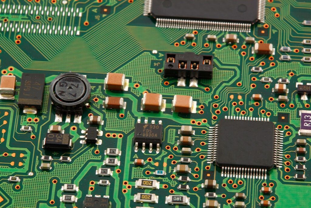
After that, we build tiny parts called transistors on the wafer. This involves removing some stuff and adding new materials to create the transistors. Now, we connect these transistors using a thin layer of metal. This step is called metallization. After connecting everything, we cut the wafer into individual chips. Each chip is then tested to make sure it works perfectly. Upon successful completion of testing, the chips are separated from the wafer chips and undergo the packaging process. Packaging serves a dual purpose, shielding the delicate chip from environmental factors and providing the necessary electrical connections for integration into electronic devices. The final products, now encapsulated in protective casings, undergo additional quality control measures before embarking on their journey to manufacturers.
Making computer chips is like a clever and intricate interplay of science and engineering. It creates the amazing technology we use every day. This process keeps getting better, and it's the reason our computers and devices keep getting faster and more connected. As we move deeper into the digital era, the people working on computer chips are at the front, leading us into the future of technology. Let's understand what is a chip? & What is a Wafer?
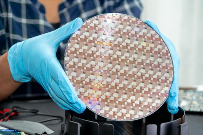
A chip, an integrated circuit that performs specific functions. These chips are crafted from semiconductor materials, predominantly silicon. They act as the brain of devices, executing tasks ranging from simple calculations to complex operations. Making a computer chip starts with a digital plan designed by engineers. They use special tools to make a detailed plan that decides how the chip's parts will be arranged and connected. It's like planning a building, where the details matter a lot. Once the plan is ready, it goes from being a virtual idea to a real guide for the next steps. The next steps involve creating masks, which are like stencils. These masks help put patterns on silicon wafers, which are like the canvas for the chip. The wafers are cut from a big piece of wafer silicon. The size of these wafers is important for making things work well. Then, an extra layer is added to the wafer to make it work even better.
After that, a special material sensitive to light is applied to the wafer. This material helps transfer the patterns from the masks to the wafer. Some areas are then etched, or sculpted, to make the wafer electronics into the right shape. Adding tiny bits of other materials in a careful way (called doping) is important for making certain parts of the chip work. Thin layers are added using special methods, making the chip more complex. The chip's design is refined further with special processes. The chip is tested to make sure it works well, and any that don't meet the standards are not used. Quality checks are very important to make sure the final chip is reliable.
Now, the chips are separated from the silicon wafers and put into protective packages. These packages keep the chips safe and help them connect to other devices. Chips are not just in phones and computers; they're used in many things like medical devices and cars. They're a big part of our daily lives. Looking ahead, the people who make chips are always coming up with new ideas to make them even better. This includes using chips for things like artificial intelligence and quantum computing.
A wafer is a thin, usually round slice of material that's shiny. It's important for making electronic chips. To make it, we go through four main steps: growing a crystal, turning it into a wafer, polishing the wafer, and getting it ready for use. First, we make a crystal with special properties. Then, we shape this crystal into a thin, round wafer with specific size and thickness. What is a Wafer? - A wafer, a thin slice from a single crystal of silicon, serves as the foundation for the intricate world of semiconductor wafers devices. Beginning as a meticulously grown crystal, the silicon ingot undergoes precision slicing and polishing to become a flat and smooth wafer electronics, crucial for subsequent manufacturing steps.
Wafer sizes, commonly 200mm and 300mm, evolve to enhance efficiency and cost-effectiveness, with consideration given to factors like production efficiency and equipment compatibility. In advanced semiconductor manufacturing, epitaxy adds a thin layer to the wafer's surface, enhancing its electrical properties for improved device performance. The wafer transforms into a wafer semiconductor device through lithography, a process involving pattern transfer using masks as stencils. Doping follows, introducing controlled impurities to modify the wafer's electrical properties, crucial for creating transistors and other components. Additional complexity arises from the deposition of thin films using techniques like chemical vapor deposition (CVD) or physical vapor deposition (PVD).
Rigorous testing identifies and eliminates defective components, ensuring the semiconductor wafers device meets quality standards. Packaging goes beyond protection, influencing performance, thermal characteristics, and overall reliability. The encapsulation process shields components while providing necessary connections for integration into electronic devices. Wafers play a pivotal role in ubiquitous wafer semiconductor wafers devices, from microprocessors in computers to memory chips in smartphones, defining our modern era. Looking forward, advancements such as 3D integration, novel materials, and advanced lithography techniques hold promise for the future of wafer electronics
and semiconductor technology. This journey, from crystal ingot to substrate, represents the fusion of scientific principles and engineering precision, propelling us into a future where semiconductor technology continues to expand possibilities.
In Conclusion, As technology continues to advance, the semiconductor industry will play an even more significant role in shaping our future. The relentless pursuit of smaller, faster, and more efficient chips will continue to drive innovation and enable new possibilities in various fields, from artificial intelligence and autonomous vehicles to healthcare and renewable energy. As we conclude our exploration of chips and wafers, it becomes evident that these small components have a monumental impact on our daily lives. From the silicon wafer manufacturers to the intricate processes of creating integrated circuits, the semiconductor wafer industry is a testament to human innovation.
The wafer semiconductor industry is vital to our modern world, powering the electronic devices we use every day. It starts with designing intricate chip blueprints using computer tools. These designs become physical patterns on silicon wafers, chosen carefully for efficiency and cost. The manufacturing journey involves adding layers to the wafer chips, creating circuitry patterns through exposure to light and chemical processes. Controlled impurities are introduced to make transistors and other components. Further layers refine the chip's design through processes like deposition, lithography, and metallization.
Testing ensures only high-quality chips progress, with strict criteria for functionality and performance. Once tested, chips are protected in casings during packaging, influencing performance and reliability. Chips power more than consumer electronics; they're crucial in servers, medical devices, and various industries. The semiconductor industry is central to progress, influencing technology and innovation. Looking ahead, the industry faces challenges like environmental concerns and ethical use of technology. While Moore's Law drives computational advancements, the industry must adapt to a changing global landscape.
- Wafer Probing: An Ultimate Guide
- Top Semiconductor Chip Manufacturers in the World
- Free Worldwide Shipping on Over 600,000 Electronics Components with HQ Online
- Free PCB Assembly Offer is Now Live: Experience Reliable PCB Assembly from HQ NextPCB
- HQ NextPCB Introduces New PCB Gerber Viewer: HQDFM Online Lite Edition
Still, need help? Contact Us: support@nextpcb.com
Need a PCB or PCBA quote? Quote now
|
Dimensions: (mm) |
|
|
Quantity: (pcs) |
|
|
Layers: |
Thickness: |
|
|
|