
Support Team
Feedback:
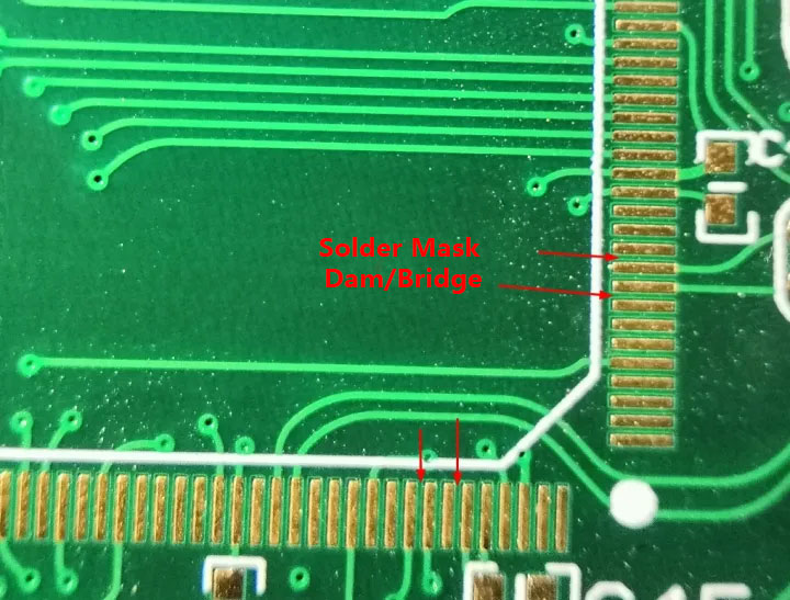
support@nextpcb.comA solder mask bridge, also known as a solder mask dam, is a small section of the solder mask layer on a printed circuit board that is left open or exposed around the perimeter of each pad or through-hole. The purpose of a solder mask bridge is to prevent the flow of solder or other conductive materials from one electrical connection to another during the assembly process. The term "green oil bridge" is sometimes used to refer to the green-colored solder mask material that is commonly used on PCBs, but this is not a widely recognized term.
By creating a small barrier, the solder mask dam ensures that the solder joints are formed only where intended, preventing electrical shorts and other types of damage that can cause electronic devices to malfunction or fail. Solder mask dams are important for ensuring the reliability and performance of electronic devices, as they protect the copper traces and other metal features from oxidation, contamination, and other forms of damage.
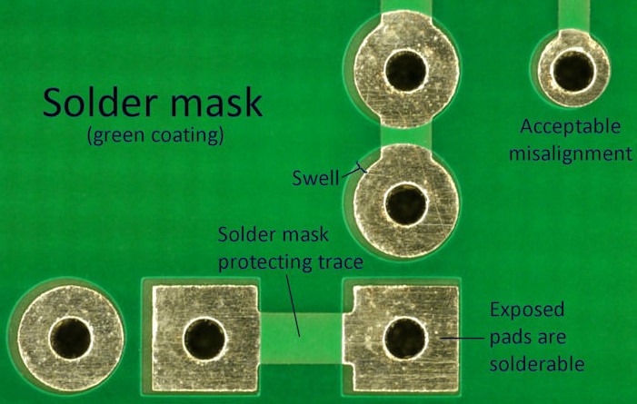
Printed circuit boards are the backbone of many electronic devices, providing a platform for electronic components to be connected and communicate with each other. The solder mask layer is a thin, uniform layer of polymer material that is applied to the surface of the board to protect the copper traces and other metal features from oxidation, contamination, and other forms of damage. The solder mask layer also serves as a barrier to prevent the flow of solder or other conductive materials from one electrical connection to another.
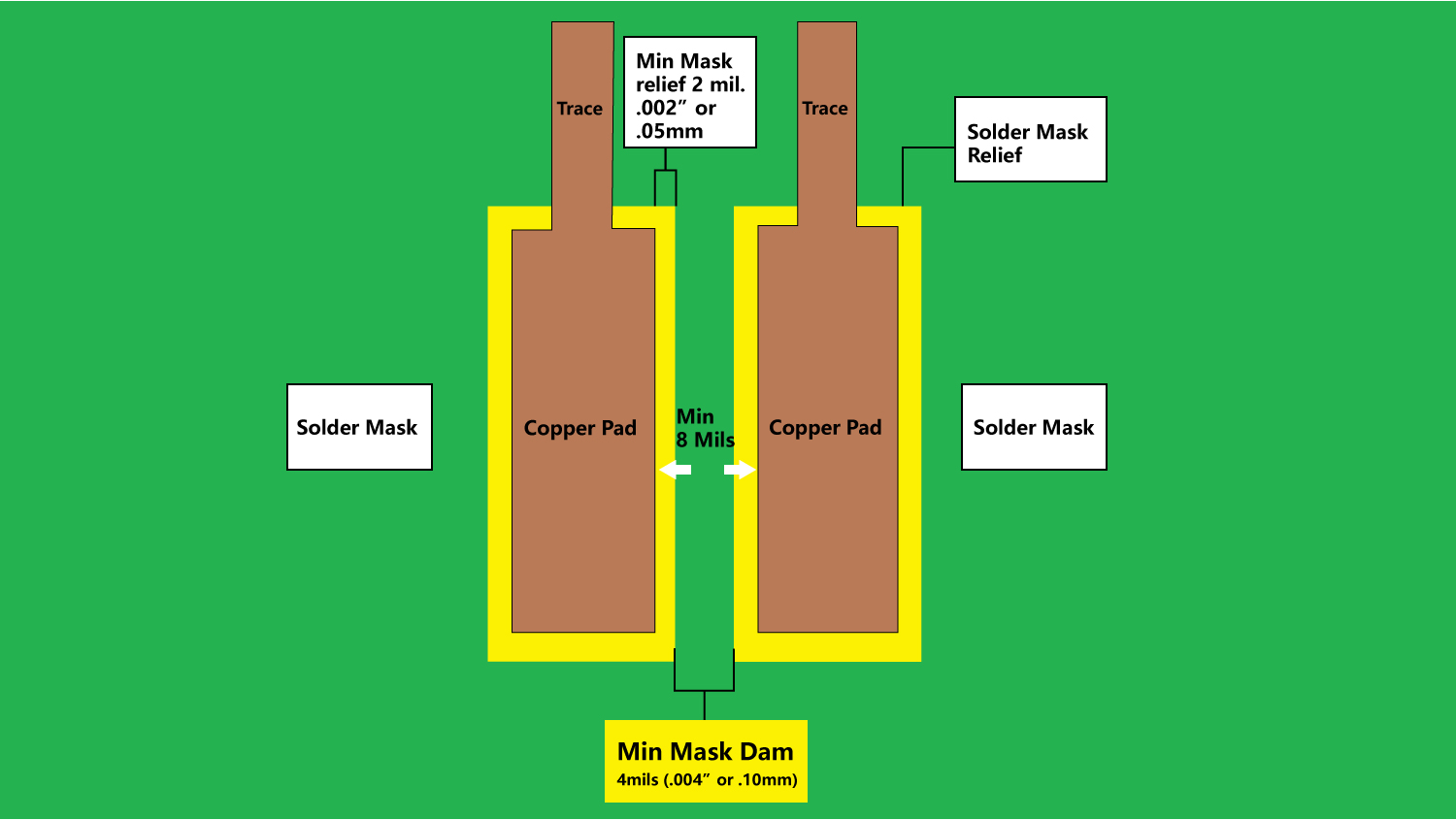
Solder mask dams are an essential feature of the solder mask layer. By creating a small barrier around each pad or through-hole, solder mask dams prevent the flow of solder outside of the intended area during the assembly process. This ensures that the solder joints are formed only where intended, preventing electrical shorts and other types of damage that can cause electronic devices to malfunction or fail.
Solder mask dams function by preventing the solder from flowing outside of the intended area during the assembly process. Without solder mask dams, solder can flow onto adjacent conductive features, causing electrical shorts or other types of damage. Solder mask dams are crucial for preventing these types of problems and ensuring the reliability and performance of electronic devices.
There are several types of solder mask dams that can be used, including open, hatched, and round dams. Each type of solder mask dam has its advantages and disadvantages, and the appropriate type should be selected based on the specific requirements of the PCB design.
Open solder mask dams are the simplest and most common type of solder mask dam. They are created by leaving a small open space around each pad or through-hole, allowing solder to flow onto the pad or through-hole without spreading to adjacent conductive features.
Hatched solder mask dams are similar to open solder mask dams, but they use a pattern of diagonal lines to create a barrier around each pad or through-hole. The diagonal lines create small gaps in the solder mask, which allow the solder to flow onto the pad or through-hole without spreading to adjacent conductive features.
Round solder mask dams use a circular shape to encircle each pad or through-hole. The circular shape creates a barrier around the pad or through-hole, preventing solder from flowing onto adjacent conductive features.
The PCB layout is an essential consideration when designing the SMD. The designer must ensure that there is enough space for the dam and that it doesn't interfere with other components or traces on the board.
Additionally, the placement of the components on the board is also important when designing the solder mask dam. The designer must consider size and shape and protect the component without obstruction.
The type of solder mask material used is also a significant consideration. The designer needs a compatible material for insulation and protection that fits the manufacturing process.
The first step in designing an SMD is to set up the design rules. We determine the minimum size and clearance for the dam and actively avoid any interference it may have with other components or traces on the board.
After setting up the design rules, the designer can actively begin placing the solder mask dam on the board. We must place the dam adequately to protect the component while ensuring it functions properly.
In short, it is significant in making PCBs for electronic devices. Additionally, it also adds a layer of protection by covering the copper traces to prevent any accidental short circuits. Furthermore, this protective layer also prevents oxidation and corrosion.
It's part of the PCB fabrication process that involves several steps, including designing the PCB layout, printing the solder mask layer, and curing it. The solder mask's thickness, color, and material type affect the PCB's performance. It is significant to consider these factors when designing the solder mask layer.
Still, need help? Contact Us: support@nextpcb.com
Need a PCB or PCBA quote? Quote now
|
Dimensions: (mm) |
|
|
Quantity: (pcs) |
|
|
Layers: |
Thickness: |
|
|
|


