Support Team
Feedback:
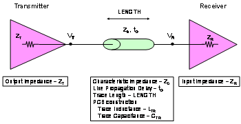
support@nextpcb.comWhen you're dealing with transmission line matching problems in your system, you need to understand the electrical impedance and characteristics of integrated circuits and PCB traces. Figure 1 shows the block diagram of a single-ended transmission line.

Figure 1 Single-ended transmission line connecting the transmitter, transmission line and receiver components
In terms of transmission lines, we can extract the IC's transmitter output impedance (ZT, Ω) and receiver input impedance (ZR, Ω) from the IC IBIS model. Many times, these integrated circuit (IC) specifications are not covered in the IC manufacturer's product specification, but you can get all of these values through the IBIS model.
You can define the transmission line with the following four parameters: characteristic impedance (Z0, Ω), board propagation delay (D, ps/in), line propagation delay (tD, seconds), and trace length (LENGTH, inches). In general, the FR-4 board has a Z0 range of 50Ω to 75Ω, while D ranges from 140 ps/in to 180 ps/in. The actual values of Z0 and D depend on the material and physical dimensions of the actual transmission line (Reference 1). The line delay (tD) on a particular board is equal to the propagation delay (D) multiplied by the length of the stitch you are using (LENGTH). All boards are calculated as:
D = 1012 Ö (CTR * LTR) or
D = 85 ps/in * Ö (er)
Z0 = Ö (LTR/CTR)
tD = D * LENGTH
When using the FR-4 board, a reasonable stripline propagation delay of 178 ps/in and a characteristic impedance of 50Ω.
The transmitter specification for signal integrity evaluation is the output impedance (ZT). When determining the output impedance, the [Pin] area in the IBIS model provides the resistance, inductance, and capacitance parasitics for each pin. After that, you can put the package capacitance together with the capacitance value of each buffer (C_comp) for a clearer understanding.
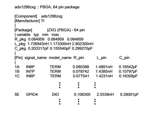
As described by [Component], [Manufacturer], and [Package] on the [Pin] keyword, the [Pin] keyword is specific to the encapsulation. You will find the package capacitor and inductor in the [Pin] keyword table because it is pin dependent. For example, in the ads129x.ibs model, Figure 2 shows where to find the L_pin and C_pin values for pin 5E (PBGA, 64-pin package) signal GPIO4.

Figure 2 List of packages for the ads1296zxg package including the C_pin value
The signal and package L_pin (pin inductance) and C_pin (pin capacitance) are 1.489 Nh and 0.28001 pF, respectively.
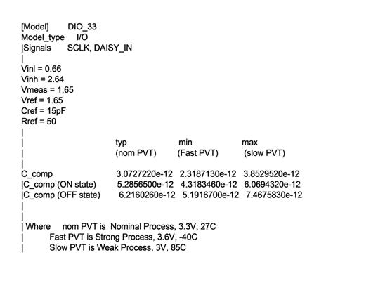
The second important capacitor value is the C_comp value below the [Model] keyword. Just as you find the correct model in the IBIS model, you will also find a list of C_comp values. Figure 3 shows an example of C_comp in the DIO_33 model.

Figure 3 ads129x.ibs, which is a list of Model DIO_33 and its associated C_comp values.
In the statement in Figure 3, the "|" symbol indicates a comment. The list of valid C_comps in this statement is:
| typ min max
| (nom PVT) (Fast PVT) (slow PVT)
C_comp 3.0727220e-12 2.3187130e-12 3.8529520e-12
Through this list, PCB designers can choose among three values. The typical value of 3.072722 Pf is the right choice during the PCB transmission line design phase.
The IBIS model provides PCB designers with some clues to perform board simulations before moving to prototype design. If you know how to find it, the IBIS model gives you the characteristic impedance and capacitance of all the pins.
Still, need help? Contact Us: support@nextpcb.com
Need a PCB or PCBA quote? Quote now
|
Dimensions: (mm) |
|
|
Quantity: (pcs) |
|
|
Layers: |
Thickness: |
|
|
|