Support Team
Feedback:
support@nextpcb.com
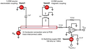
Figure 1 Coupling medium for conductive EMI signals
Conductive EMI interference is the result of the normal operation of the switching circuit and the parasitic capacitance and inductance. Figure 1 shows some of the EMI sources that will enter your PCB traces. Vemi1 is derived from a switching network such as a clock signal or a digital signal trace. The coupling of these sources of interference is through the parasitic capacitance between the traces. These signals bring current spikes into adjacent PCB traces. Similarly, Vemi2 is derived from a switching network or from an antenna on the PCB. The coupling of these sources of interference is through the parasitic inductance between the traces. This signal brings voltage disturbances into adjacent PCB traces. Every three EMI sources come from adjacent wires within the cable. Signals propagating along these wires can create crosstalk effects.
The switched mode power supply produces Vemi4. Interference from the switched-mode power supply resides on the power trace and appears as a Vemi4 signal.
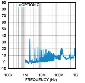
Switched-mode power supply (SMPS) circuits present opportunities for the formation of conductive EMI during normal operation. The "on" and "off" switching operations within these supplies produce a strong discontinuous current. These discontinuous currents are present at the input of the buck converter, at the output of the boost converter, and at the input and output of the flyback and boost topology. The discontinuous current caused by the switching action produces a voltage ripple that propagates through the PCB traces to other parts of the system. The input and/or output voltage ripple caused by the SMPS can jeopardize the operation of the load circuit. Figure 2 shows an example of the frequency composition of a DC/DC buck SMPS input operating at 2 MHz. The basic frequency composition of SMPS conducted interference ranges from 90 – 100 MHz.

Figure 2 DC/DC Buck Converter: Switching Frequency = 2MHz
Conductive EMI measurements with 10 μF filters for input and output pins.
There are two types of conducted interference: differential mode interference and common mode interference. Differential mode interference signals appear between the input terminals of the circuit, such as signal and ground. Current flows through the two inputs of the same phase. However, the current input size 1 is equal to the 2nd, but the direction is opposite (differential reference). The loads at these two inputs form a voltage that varies with current strength. This voltage change between stitch 1 and the differential reference creates interference or communication errors in the system.
Common mode interference occurs when you add a ground loop or a bad current path to the circuit. If there is a source of interference, common mode current and common mode voltage are formed on trace 1 and trace 2, and the ground loop acts as a common mode interference source. Both differential and common mode interference require special filters to handle the adverse effects of EMI interference.
Still, need help? Contact Us: support@nextpcb.com
Need a PCB or PCBA quote? Quote now
|
Dimensions: (mm) |
|
|
Quantity: (pcs) |
|
|
Layers: |
Thickness: |
|
|
|