
Support Team
Feedback:
support@nextpcb.comAntennas constructed on a Printed Circuit Board (PCB) substrate use the board's conductive traces and components as their conductors. This PCB antenna is popular because of its small size, inexpensive price, and simple integration into a wide variety of electrical products. A variety of various uses are possible for printed circuit board antennas due to their versatility.
A PCB antenna's portability is one of its main selling points. PCB antennas can be made to take up a minuscule amount of real estate on a PCB, making them ideal for compact devices. In addition to reducing the size and complexity of the device, PCB antennas do away with the requirement for external antennas. PCB antennas are advantageous because of their inexpensive price. The antenna can be made with no extra parts or materials by fabricating it directly onto the PCB substrate. The low cost per unit means that PCB antennas are a good choice for mass production.
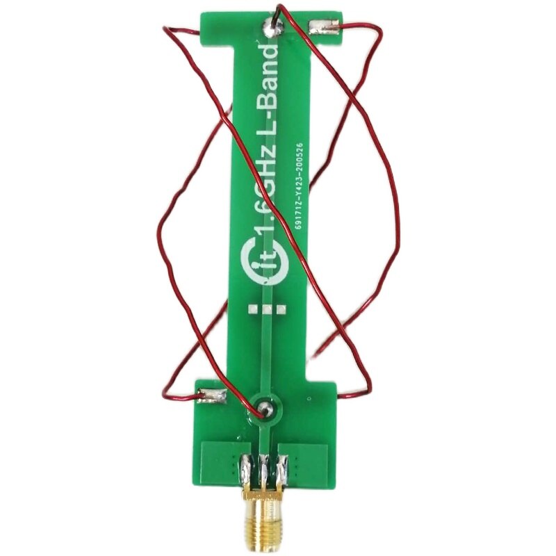
Many PCB antenna varieties exist, each with its own set of pros and cons. Common PCB antennas include monopole, dipole, patch, and loop designs. Selecting the right antenna for a given application requires thinking about factors like radiation pattern, gain, and bandwidth, among others, for each of these antenna types. Steps in designing a printed circuit board antenna include analyzing the antenna's intended use, selecting an appropriate antenna type, sketching out the antenna's physical layout, maximizing impedance matching, fine-tuning the radiation pattern, fabricating the antenna, and finally testing its efficacy.
There are several steps to designing a Printed Circuit Board (PCB) antenna, and each one is important to how well the antenna works as a whole. In this intro, we'll give a quick rundown of the steps that go into making a PCB antenna.
The first step in designing a Printed Circuit Board (PCB) antenna is to figure out what the application needs. The type of antenna, frequency range, radiation pattern, gain, and other performance metrics needed will depend on the exact needs of the application. Here are some things to think about when figuring out what a PCB antenna design needs to do:
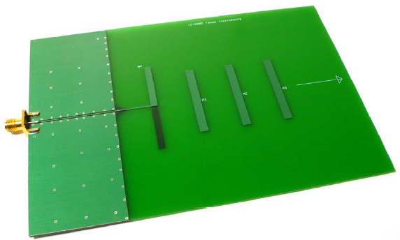
The design of a PCB antenna relies heavily on the selection of the optimal antenna type. The requirements of the application and the intended antenna performance characteristics will determine the antenna type selected. Below, we outline the types of PCB antennas and their defining features.
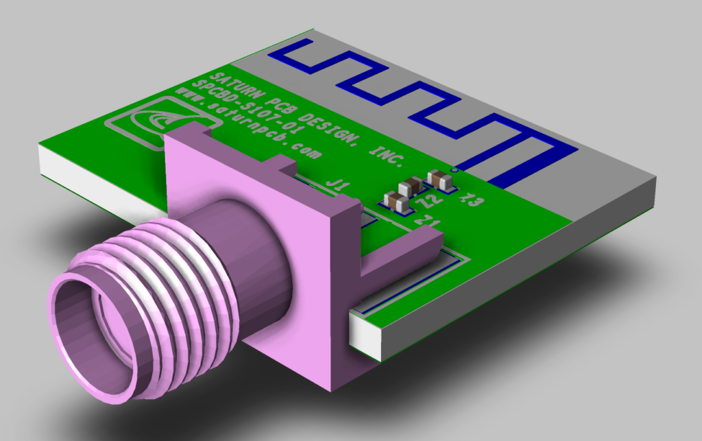
Monopole antennas have just one radiating element and get their power supply from a coaxial cable. The radiation pattern of a monopole antenna is uniform in all directions. Broad coverage applications, such as wireless communication systems, are common users of these antennas.
Two radiating elements connected through coaxial cable make up a dipole antenna. In FM radio and Wi-Fi networks, people frequently employ dipole antennas, which, like monopole antennas, are omnidirectional.
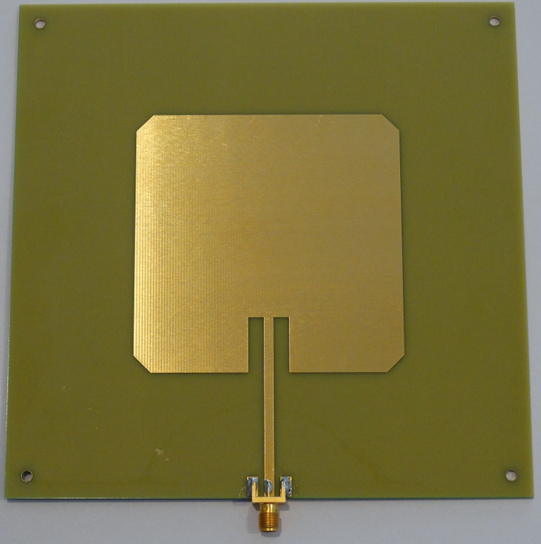
Placing a radiating element on top of a ground plane is the defining characteristic of the patch antenna, which is a type of antenna. Directional patch antennas only broadcast in one direction. GPS systems and wireless routers are just two examples of commonplace uses.
Connecting a loop of wire to a source of power, typically a coaxial cable, creates a loop antenna. Like dipole antennas, loop antennas allow for directional pointing, rendering them beneficial for RFID and AM radio.
The Yagi antenna is a type of directional antenna that uses a dipole and one or more parasitic elements to focus radio waves in a certain direction. It finds widespread use in fields like radio and television transmission.
In a helical antenna, one coils the wire into a helix shape, creating a directional antenna. It finds widespread use in fields like satellite communication and global positioning system technology.
There are other alternative PCB antenna designs, each with its own set of pros and cons. When deciding on an antenna type, one should take into account factors such as frequency range, gain, radiation pattern, and physical dimensions. To get the desired performance characteristics, it may be necessary to use a combination of antenna types.
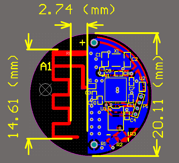
The layout of the antenna determines its radiation pattern, efficiency, and other performance qualities. There are several things to think about while planning an antenna arrangement.
The placement of the feed point is an important consideration. The placement of the feed point, where the signal is first delivered into the antenna, can have a major effect on the antenna's performance. It is essential to position the feed point in a way that maximizes the radiation efficiency of the antenna. The dimensions and contours of the ground surface are still other elements to think about. The ground plane is crucial to the antenna because it provides a foundation for designing the radiation pattern. Modifying the size and form of the ground plane can fine-tune the radiation pattern of the antenna.
When planning the antenna's layout, don't forget about the corresponding networks and filters! Including these parts in the antenna design can boost its functionality and efficiency.
Understanding the needs of the application and the antenna's performance characteristics is crucial when creating the antenna layout for a PCB antenna design. An effective antenna architecture that satisfies the required parameters can be designed with this info in mind.
To maximize power transfer and reduce signal reflections, match the antenna and feeding circuit impedances.
Antenna efficiency and signal-to-noise ratio are both diminished by mismatched impedance.
An impedance-matching network is a common method for achieving impedance matching. Connected between the feeding circuit and the antenna, passive components like resistors, capacitors, and inductors form an impedance-matching network. The impedance of the antenna and the feeding circuit can be matched by adjusting these parts. Impedance matching can also be accomplished by making adjustments to the antenna's physical size. The antenna's impedance can be tuned to the feeding circuit by modifying its dimensions (length, width, and thickness). However, this method can be more difficult and time-consuming than using an impedance-matching network. Simulation software can also be used to optimize impedance matching. The software can simulate the performance of the antenna under different impedance conditions, allowing for adjustments to be made before fabrication.
Overall, optimizing impedance matching is an essential step in the design of a PCB antenna. By achieving a good impedance match, the antenna can perform at its best, ensuring maximum efficiency and signal quality.
The simulation allows engineers to predict the performance of the antenna and make necessary adjustments before the physical antenna is fabricated. There are various simulation tools available for designing PCB antennas, including ANSYS HFSS, CST Microwave Studio, and FEKO. These software packages allow engineers to model the electromagnetic behavior of the antenna and visualize the radiation pattern, gain, and other performance metrics.
Simulating an antenna and its environment requires a 3D model. The model incorporates antenna dimensions and PCB components that may affect antenna performance. Simulation software solves electromagnetic equations numerically and predicts antenna performance.
Engineers can optimize antenna design during simulation. Changes in antenna dimensions or component placement can change radiation patterns and gain. Engineers can determine the best antenna design by simulating design iterations. After the simulation, the engineer can compare the antenna's performance to the desired requirements. The engineer can tweak the design and repeat the simulation until the antenna meets the specified criteria.
PCB antenna design requires antenna simulation. Engineers can optimize antenna performance using simulation tools.
One of the most important steps in designing a PCB antenna is fine-tuning its radiation pattern to achieve the required performance.
How an antenna disperses its radiated electromagnetic field is known as its radiation pattern.
The radiation pattern of a PCB antenna is influenced by several factors, including the shape and size of the antenna, the location of the feed point, and the presence of any surrounding objects or structures. Adjusting the radiation pattern involves tweaking these factors to achieve the desired radiation pattern.
One common technique for adjusting the radiation pattern of a PCB antenna is to use simulation software. This software can simulate the electromagnetic field radiated by the antenna and predict the resulting radiation pattern. By tweaking the dimensions of the antenna and the placement of components, the radiation pattern can be adjusted to meet the desired specifications.
Another technique for adjusting the radiation pattern is to use a technique called beamforming. Beamforming involves adjusting the phase and amplitude of the signals fed to the antenna elements to steer the radiation pattern in a specific direction. This technique can be used to create directional antennas with high gain and narrow beam widths.
Modifying a PCB antenna's radiation pattern involves a number of parameters and is not a simple task. Better signal quality, longer range, and more efficiency can all result from fine-tuning the antenna's emission pattern.
Once the PCB antenna design is finalized, the next step is to fabricate the antenna. Fabrication involves transferring the antenna design onto the PCB substrate using standard manufacturing techniques. The manufacturing process typically involves the following steps:
Substrate preparation: The PCB substrate is prepared by cleaning and surface treating it to ensure good adhesion of the conductive material.
Conductor deposition: Using a process such as electroplating or sputtering, one deposit a layer of conductive material, typically copper, onto the substrate. One deposit the conductor in the shape of the antenna design.
Etching: Etching removes the areas of the conductor that are not part of the antenna design. The etching process typically involves immersing the PCB substrate in a solution of an etchant such as ferric chloride.
Resist removal: Once the conductor has been etched, any remaining resist material is removed from the substrate using a solvent or plasma.
Finishing: The finished antenna may require additional processing, such as adding a protective coating or soldering any necessary components.
The method used to create the antenna can impact its performance. Factors such as the thickness of the conductor and substrate can impact the antenna's impedance. To build the antenna to the required standards, it is essential to tightly manage the fabrication process. To recap, a printed circuit board antenna is made by depositing a layer of conductive material onto a substrate, then etching the conductor to form the antenna design, and applying any necessary finishes. Fabrication is a crucial stage in PCB antenna design since it can have a major effect on antenna performance.
There are several benefits of using a Printed Circuit Board (PCB) antenna in electronic devices, including:
Small size: Custom-designed PCB antennas take up minimal space on a PCB, which is ideal for devices with limited available space.
Low cost: Fabricating the antenna directly on the PCB substrate eliminates the need for any additional components or materials, simplifying the design and reducing costs. This makes PCB antennas an attractive option for high-volume production runs.
Incorporating PCB antennas within a device is more simpler than doing so with external antennas, which can add unnecessary bulk.
Incorporating PCB antennas directly into the PCB layout can streamline the design process.
Manufacturers can customize PCB antennas to work for a wide range of frequencies.
Due to their resistance to moisture, dust, and other environmental factors, PCB antennas are more reliable.
In conclusion, PCB antennas are compact, inexpensive, and easy to integrate into a variety of electronic equipment. As electronics become smaller and more complex, the usage of PCB antennas increases.
Developing a PCB antenna requires assessing application requirements, choosing the right antenna type, planning the antenna layout, optimizing impedance matching, changing the radiation pattern, producing the antenna, and testing its performance.
PCB antennas are compact, cheap, easy to integrate, customizable, reliable, and perform well. PCB antennas appeal to electronic device manufacturers because they can customize them for a specific application.
Technology will drive demand for smaller, more complicated gadgets. PCB antennas are becoming increasingly popular due to their cost-effectiveness and ease of integration into electronic products, making them a viable solution to meet this need.
Still, need help? Contact Us: support@nextpcb.com
Need a PCB or PCBA quote? Quote now
|
Dimensions: (mm) |
|
|
Quantity: (pcs) |
|
|
Layers: |
Thickness: |
|
|
|


